Good day. Today my post is about voltage stabilizers. What is it? First of all, any electronic circuit needs a power source to work. Power sources are different: stabilized and unstabilized, direct current and alternating current, pulse and linear, resonant and quasi-resonant. Such a wide variety is due to the different circuits from which electronic circuits will operate. Below is a comparison table of power supply circuits.
Parametric with zener diode, parallel
Surge Protectors: Less Deception Surge Protectors are a little better than stabilizers, but they're far from real saviors. The vast majority of them do not fix problems in electrical network, transmitting the same noise it receives from the outlet to connected devices. At least that's what happens with the cheapest filters on the market.
What is true salvation? Unfortunately, the alternative that actually works is a bit more expensive than stabilizers and surge protectors. We're talking about riots. This type of electrical component provides protection on four different fronts. Surge protection; Voltage drop protection; Power outage protection; Oscillation frequency protection. Within a segment without discontinuities, it is still possible to divide them into two different types.
For nutrition electronic circuits, which do not require high stability of the DC supply voltage or high output power, it is advisable to use simple, reliable and cheap linear voltage sources. The basis of any linear voltage source is parametric voltage regulator. The basis of such devices is an element with a nonlinear current-voltage characteristic, in which the voltage on the electrodes depends little on the current flowing through the element. One of these elements is zener diode.
Large servers are accustomed to using online breaks, which are the most complete in terms of preventing electrical problems. This type of device is in a constant state of energy change as it powers computers with battery life at the same time as it is being charged with power from outlets.
Why do we need ferroresonant models?
According to the above Professor Eduardo Romaneli, they are non-stop online, which makes security and stability more reliable. The problem, as already mentioned, is the high cost to acquire it. For this reason, it is estimated that most non-working ones are installed in energy servers and power plants for companies.
zener diode represents a special group, the mode of operation of which is characterized by the reverse branch of the current-voltage characteristic in the breakdown region. Let us consider in more detail the current-voltage characteristic of the diode.
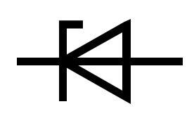
The principle of operation of the zener diode
When the diode is turned on in the forward direction (anode - "+", cathode - "-"), then it freely begins to pass current at voltage U then, and when turned on in the opposite direction (anode - “-”, cathode - “+”), only current I arr, which has a value of several µA. If you increase reverse voltage U arr on the diode up to a certain U arr.max values an electrical breakdown of the diode will occur and if the current is sufficiently driven, then a thermal breakdown occurs and the diode fails. The diode can be made to work in the electrical breakdown region by limiting the current that passes through the diode (the breakdown voltage for different diodes is 50 - 200 V).
However, it is noted that in domestic electrical installations it is much more recommended to use a stand-alone UPS. But this is only in places where the power grid is too unstable, causing signal spikes that can damage electronic devices. In more stable networks, it is sufficient to use surge protectors with support for electromagnetic filters.
Take advantage of the comment space to tell us if you were aware of the insufficiency of these devices in controlling the electrical voltage that reaches our homes. It also takes into account which electronic devices are connected to the stabilizer in order to prevent discharges from affecting operation.
The zener diode is designed in such a way that its current-voltage characteristic in the breakdown region is highly linear, and the breakdown voltage is fairly constant. Thus, we can say that voltage stabilization by a zener diode is carried out during its operation. on the back branch current-voltage characteristics, in the same area straight branch A zener diode behaves similarly to an ordinary diode. The zener diode is designated as follows
Schematic diagram of the relay device
Before reaching electrical outlets electric power moves to long distances and change in characteristics. While generation, transmission, and distribution systems are designed to provide uninterrupted power, the sheer number of users and equipment connected to this network, combined with the lack of maintenance on cables and transformers, can create short circuits, blackouts, power surges, and voltage surges in the electrical current.
The main parameters of the zener diode
Consider the main zener parameters according to its volt-ampere characteristic.

Stabilization voltage U st determined by the voltage on the zener diode during the flow stabilization current I st. Currently, zener diodes are produced with a stabilization voltage from 0.7 to 200 V.
Disturbances in the power supply network of the public network, even imperceptible to humans, can cause damage to electrical and electronic equipment, whether energized or not, simply because they are connected to electrical outlet. inadequate electrical installations such as low level wiring for the required voltage or lack of grounding can also cause electronics to malfunction.
This is due to the fact that electrical networks deliver energy with a voltage of 110 volts and 220 volts AC. To ensure proper power supply to computers, there is a power supply that supplies each component. These sources are designed to receive electricity from a given voltage.
The maximum allowable direct stabilization current I st.max limited by value maximum allowable power dissipation P max, which in turn depends on the temperature environment.
Minimum stabilization current I st.min is determined by the minimum value of the current through the zener diode, at which the operability of the device is still fully preserved. Between the values of I st.max and I st.min, the volt-ampere characteristic of the zener diode is the most linear and the stabilization voltage changes slightly.
Such changes can be of several types: overvoltage, undervoltage, transients, voltage drop and peak voltage. There are two types of devices used on the market designed to protect computers and peripherals from these problems, line filters and voltage regulators, the features of which are completely different.
In addition to removing noise and spikes, line filters have other primary purposes. This is possible because most linear filters have circuit breaker responsible for turning off the power if the total current required by the equipment exceeds rated current. In the case of fuse-protected devices, in the event of an overvoltage, it will melt, requiring it to be replaced in order for the line filter to work again.
Zener diode differential resistance r ST- the value determined by the ratio of the stabilization voltage increment on the device ΔU CT to the small increment of the stabilization current that caused it Δi CT .
A zener diode connected in the forward direction, like a conventional diode, is characterized by the values permanent direct voltage U pr and maximum allowable direct current I pr.max.
Since the market for line filters is large, there are many manufacturers who have put products on sale that do not bring all the protection components necessary for good EMI and surge filtering. Some devices don't even have filter components, working as a simple extension.
Cheap line filters do not have EMC filtering components, although they do have at least one varistor, a small electronic component that provides protection against short-term electrical discharges. Good line filters have both varistors and EMC filtering components.
Parametric Stabilizer
The basic circuit for switching on a zener diode, which is a circuit parametric stabilizer, as well as a reference voltage source in other types of stabilizers is given below.
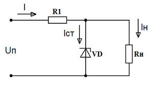
This circuit is a voltage divider, consisting of ballast resistor R1 and zener diode VD, parallel to which the load resistance R N is connected. Such a voltage stabilizer ensures the stabilization of the output voltage when the supply voltage U P and the load current I N change.
How to buy a line filter - If you are really concerned about protecting your equipment, you should not save money when buying a line filter. We recommend choosing one that has at least three varistors. Look for the line filter with the lowest activation voltage - this setting will be described as "clamp voltage". The activation voltage is the voltage at which the varistors start to operate. Ideally, they start working at the moment when the peak voltage occurs.
Another one important detail is the response time, which is the interval required for the line filter to start working when a voltage spike is detected. There is still peak current, which is the maximum peak current that varistors can handle without burning.
Consider principle of operation of this scheme. Increasing the voltage at the input of the stabilizer leads to an increase in the current that passes through the resistor R1 and the zener diode VD. Due to its current-voltage characteristic, the voltage at the zener diode VD will practically not change, and, accordingly, the voltage at the load resistance R n too. Thus, almost all of the voltage change will be applied to the resistor R1. Thus, it is quite easy to calculate the necessary circuit parameters.
And finally, the level of energy absorption is measured in joules. It shows the amount of peak power that the line filter can support before burning your varistors. Stabilizers. The second type of protection commonly used is voltage regulators. They are designed to protect electronics from sudden voltage changes such as overvoltage and undervoltage. Its function is to regulate the electrical voltage that comes from the concessionaire's network and deliver to the computers a sufficient and constant voltage level required by the power supplies.
Calculation of the parametric stabilizer.
The initial data for the calculation for the calculation of the simplest parametric voltage stabilizer are:
input voltage U0;
output voltage U1= U st - stabilization voltage;
output current IH= IST ;
For example, take the following data: U0 = 12 V, U1 = 5 V, I H = 10 mA = 0.1 A.
A stabilizer is a device that corrects voltage differences in the network. That is, they regulate the voltage of the energy, so that the connected equipment receives energy closer to ideal. This means that if the grid is low, the stabilizer picks it up and keeps the voltage within acceptable limits.
The computer and all its peripherals must be connected to the stabilizer. However, it is important to note that the sum of the rated power values of the equipment connected to the stabilizer cannot be greater than the rated power. According to Soares, ideal solution to connect the equipment to the electrical network to ensure the best protection is: a socket, a line filter, a stabilizer and, in this case, a computer and its peripherals.
1. According to the stabilization voltage, we select a zener diode of the BZX85C5V1RL type (U st \u003d 5.1 V, differential resistance r st \u003d 10 Ohms).
2. Determine the required ballast resistance R1:
3. Determine the stabilization coefficient:
4. Determine the efficiency
Increasing the power of the parametric stabilizer
The maximum output power of the simplest parametric voltage regulator depends on the values of I st.max and P max of the zener diode. The power of a parametric stabilizer can be increased if a transistor is used as a control component, which will act as a DC amplifier.
Adjustable voltage regulator circuit
Additional protection. If you want to provide even more protection for your computer equipment, it is better to purchase a power supply. Also known as uninterruptible power supplies or UPSs, these devices provide power to the computer and peripherals in the event of a power failure and provide complete protection against problems ranging from small interruptions of a fraction of a second to complete shutdown, as well as against noise, overvoltage and undervoltage.
How does a zener diode work
These devices can work for a few minutes so that the user can shut down the computer normally without losing data, in which case they are called short-lived, as far as they can work for a long time. Its autonomy depends on the power of your batteries, as well as on the amount of equipment connected to it.
Parallel Stabilizer
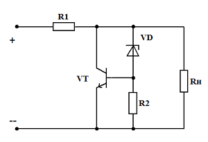
Scheme of PSN with parallel connection of a transistor
The circuit is an emitter follower, the load resistance R H is connected in parallel with the transistor VT. The ballast resistor R1 can be included in both the collector and emitter circuits of the transistor. The load voltage is
Cabinets with galvanized steel structure and front, side and cover profiles, finished with electrostatic powder painting. Transformers made of grain-oriented sheet steel impregnated with vacuum and pressure.
Allows you to reprogram sensor settings and other parameters; Measurements: Voltages between phases and phase and neutral at the input and output, currents in the input and output phases, output frequency, internal temperature and power per phase at the output; Commands Operating modes: stabilizer or bypass. Indicates whether the through passage is manual or automatic, and whether it has been activated by the user on the panel, serial or auxiliary input; Alarm: high and low output voltage, high and low input voltage, overload, frequency, high internal temperature; Readings: On, Maintenance, Bypass, Normal, High, Low, and Overload; Other features: error log with date and time. During heatwaves, temperature records, and subsequent electrical outages, we want to clear doubts about two important protective devices from falls, peaks and lack of electricity.
The scheme works as follows. With an increase in current through the resistor R H, and, accordingly, the voltage (U1 \u003d U CT) at the output of the stabilizer, the base-emitter voltage (U EB) and collector current I K increase, since the transistor operates in the amplification region. An increase in the collector current leads to an increase in the voltage drop across the ballast resistor R1, which compensates for the increase in voltage at the output of the stabilizer (U1 = U CT). Since the current I ST of the zener diode is simultaneously the base current of the transistor, it is obvious that the load current in this circuit can be h 21e times greater than the simplest scheme parametric stabilizer. Resistor R2 increases the current through the zener diode, ensuring its stable operation at the maximum value of the coefficient h21e, the minimum supply voltage U0 and the maximum load current I H.
This equipment provides more complete and effective protection than a line filter. It is responsible for maintaining a normalized output voltage, converting high and low voltages into constant voltages, functioning as a kind of funnel.
The stabilizer tries to maintain a constant and stable voltage, that is, if there are peaks in the electrical network, or there is an increase or decrease in voltage, the equipment comes into play and compensates for this difference. It also has varistors and fuses. His work is simple but very useful.
The stabilization coefficient will be equal to
where R VT is the input impedance of the emitter follower
where Re and R b are the emitter and base resistances of the transistor.
The resistance Re depends significantly on the emitter current. With a decrease in the emitter current, the resistance Re increases rapidly and this leads to an increase in R VT , which worsens the stabilizing properties. Reducing the value of Re can be achieved through the use of powerful transistors or compound transistors.
Its function is very similar to that of a bodyguard, in case of a very strong change electric current it is lit so as not to damage the computer. In many cases, a simple fuse changes "revives" the stabilizer. A comparison made by a Protestant failed to cite 7 out of 8 brands sold in the country. These stabilizers did not fulfill their main function: they stabilized the tension. However, for optimal performance of the appliance, it must be connected to an electrical network that has an independent earth circuit.
But still, there are stabilizers for sale that really give a report, but a little more expensive. UPS - best system protection and the most complete of all. This is because the UPS has a battery that is charged when the mains is working normally. This battery has a range that it keeps a connected computer at. Therefore, it is not recommended to use the computer as if nothing happened.
Series stabilizer
Parametric Voltage Stabilizer, the circuit of which is presented below, is an emitter follower on a transistor VT with a series-connected load resistance R H . The source of the reference voltage in this circuit is the zener diode VD.
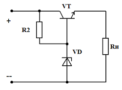
Scheme of the PSN with a serial connection of the transistor
Stabilizer output voltage:
The scheme works as follows. With an increase in current through the resistor R H, and, accordingly, the voltage (U1 \u003d U ST), at the output of the stabilizer, the opening voltage UEB of the transistor decreases and its base current decreases. This leads to an increase in the voltage at the collector-emitter junction, as a result of which the output voltage practically does not change. The optimal value of the reference zener diode current VD is determined by the resistance of the resistor R2 included in the power supply circuit U0. At a constant value of the input voltage U0, the base current of the transistor I B and the stabilization current are interconnected by the relation I B + I ST = const.
Circuit stabilization factor
where R k is the collector resistance of the bipolar transistor.
Usually kST ≈ 15…20.
Parametric Stabilizer Stabilization Coefficient voltage can be significantly increased by introducing a separate auxiliary source with U'0 > U1 into its circuit and using a composite transistor.
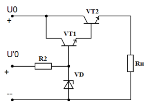
PSN circuit with a composite transistor and a zener diode powered from a separate voltage source
Theory is good, but theory without practice is just shaking the air.
VOLTAGE AND CURRENT
5.1. GENERAL INFORMATION
For normal operation communication devices, it is necessary that the supply voltage or current consumed by these devices be constant. And the voltage or current at the output of rectifiers, converters constant voltage or batteries change over time over a wide range under the influence of destabilizing factors: fluctuations in the supply voltage and changes in the load at the output of the rectifier, as well as changes in ambient temperature, a decrease in the voltage of the batteries during their discharge, etc.
The voltage of industrial AC networks supplying rectifiers, according to GOST 5237-69, can vary within -15 ... + 5% nominal value. And for the normal operation of communication devices, the change in voltage or current of the power supply should not exceed 5 ... 0.1% of its nominal value.
Stabilizers are used to reduce the influence of destabilizing factors. Voltage or current stabilizer A device is called a device that automatically maintains a constant voltage or current on the load with a given degree of accuracy when destabilizing factors change.
The impact of destabilizing factors can occur in time both slowly and very quickly - abruptly. Therefore, the stabilizers must act automatically.
Depending on the type of stabilized voltage or current, stabilizers are divided into direct voltage (current) stabilizers and stabilizers AC voltage(current). According to the method of stabilization, they are divided into parametric, compensation and impulse ones.
Currently, compensating voltage (current) stabilizers on semiconductor devices are most often used, which in turn are divided according to the features given below.
According to the method of switching on the regulating element and the load: with series and parallel connection. According to the operating mode of the regulating element: with continuous and pulse regulation.
The quality of the stabilizer is characterized by stabilization coefficients, which show how many times the relative change in the output voltage (current) is less than the relative change in the input voltage:
At I nom = const.
![]() ,
,
D U in = U input max-U input min,
D U out = U out. max-U out. min,
D I in = I input max-I input min,
D I out = I out. max-I out. min.
An important parameter of the stabilizer is the temperature coefficient for voltage TKN, or g n, showing the change in output voltage with a change in ambient temperature at constant input voltage (U in \u003d const) and load current (I n \u003d const).
The energy indicator of the quality of the stabilizer is the efficiency (h), equal to the ratio of the active power given by the stabilizer to the load, to the active power consumed by the stabilizer from the network: h = P out / P in.
Stabilizer internal resistance r i, is equal to the ratio of the output voltage increment D U out to load current increment D I n at constant input voltage U in = const, r i= D U out /D I n.
in voltage stabilizers internal resistance can reach thousandths of an ohm.
5.2. PARAMETRIC STABILIZERS
Parametric Such a stabilizer is called, in which voltage (current) stabilization is carried out by using the properties of the nonlinear elements included in its composition. In parametric stabilizers, the destabilizing factor (change in the input voltage or load current) directly affects the non-linear element, and the change in the output voltage (or current) relative to the set value is determined only by the degree of nonlinearity of the current-voltage characteristics of the non-linear element.
Parametric AC voltage stabilizer on a saturated core inductor. Parametric stabilization of alternating voltage is carried out using elements that have a non-linear current-voltage characteristic for alternating current. Such a characteristic (Fig. 5.1) has a choke operating in the saturation mode of the magnetic circuit. The working section of the throttle characteristic is a non-linear section ab corresponding to the saturated state of the magnetic wire.
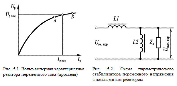
In the stabilizer circuit, a saturated choke L2 switched in parallel with the load Z n (Fig. 5.2). A choke is used as a ballast resistance L 1, operating in the saturation mode of the magnetic circuit and having a linear current-voltage characteristic.
The principle of operation of the scheme is as follows. With an increase in the AC voltage at the input of the stabilizer U output AC will increase the output voltage U AC output on load and ballast line choke L 1. The current through the saturated inductor will rise sharply. But at the same time, the voltage drop across the throttle L 1 rise while on throttle L 2 and load Z n will increase slightly. With a decrease in the input voltage, the stabilization processes occur similarly.
Advantages of such a stabilizer:
simplicity of the device;
large operating voltage range
Flaws:
low efficiency (0.4 ... 0.6), since stabilizers operate at high currents;
low power factor - 0.6;
low stabilization factor due to high dynamic resistance R d ( To st<10);
distortion of the shape of the AC voltage curve on the load;
large weight and dimensions.
5.3. FERRORESONAL STABILIZER
AC VOLTAGE
In a ferroresonant regulator in parallel with a saturated choke L 2 turn on the capacitor FROM(Fig. 5.3). Loop resonant frequency L 2C close to the frequency of the stabilized variable voltage, but not equal to it.
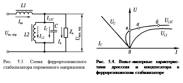
The principle of operation of a ferroresonant AC voltage regulator can be explained using the current-voltage characteristics of the inductor L 2 and capacitor FROM shown in fig. 5.4. By geometric addition of stresses U L2 and U C we get the voltage curve on the circuit L 2C. With a low input voltage, the inductor is unsaturated, its inductance is large and the resulting current has a capacitive character (0 in in fig. 5.4). At resonance of currents in the circuit L 2C(dot in) resulting current through the loop L 2C will be equal to zero. With a further increase in the input voltage, the current through the circuit has an inductive character (section wb). In this section of the characteristics, with a sharp increase in current, the voltage on the circuit, and, consequently, on the load, changes slightly.
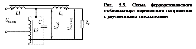
To improve the quality indicators of the stabilizer, the ferroresonant stabilizer circuit is supplemented with another inductor winding. It is located on the magnetic circuit of an unsaturated choke L1(Fig. 5.5). Compensation choke winding L to turn on so that the voltage drop across it is directed opposite to the voltage on the circuit U L 2C. In this case, the resulting voltage at the output will be the sum of the voltages on the circuit and the compensation winding U you x.lane = L L 2 C+U k. Therefore, the change in the output voltage D U you x.lane =D U L 2 C+D U k will be less than that taken only from the contour L2C. Throttle L2 connected as a step-up autotransformer to reduce the capacitance of the capacitor FROM and getting more voltage at the output of the stabilizer.
Advantages of ferroresonant stabilizers:
high efficiency (0.85…0.9) and power factor (up to 0.9);
high voltage stabilization factor (up to 40);
wide power range;
long service life;
simplicity of the device and reliability of work;
resistance to mechanical stress.
Flaws:
a significant change in the output voltage from a change in the input voltage as a result of the dependence of reactances on frequency;
the presence of electromagnetic interference (large stray fields of inductances);
large dimensions and weight;
distortion of the shape of the stabilized voltage on the load.
5.4. DC VOLTAGE REGULATORS
In parametric DC voltage stabilizers, resistors are used as linear elements, and semiconductor (silicon) zener diodes and semiconductor stabistors are used as nonlinear elements.
silicon zener diode is a planar diode. Its current-voltage characteristic is shown in fig. 5.6, a. The working part of the characteristic is the reverse branch in the region
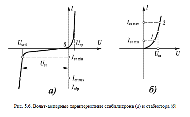
breakdown, where a slight increase in voltage causes a significant increase in current through the zener diode. However, electrical breakdown of the junction does not damage the zener diode. Thus, if the zener diode is turned on in the opposite direction, then with significant changes in the current flowing through it (from I st min up to I st max) the voltage on it remains almost constant. If the reverse voltage on the zener diode exceeds the allowable one, the power released in the zener diode exceeds the allowable one. As a result, in this case, the electrical breakdown turns into thermal, and then the p-n junction is irreversibly destroyed.
Stabistor is a semiconductor device, the voltage on which in the forward direction changes slightly with significant changes in the current flowing through it. The stabistor is included in the stabilization circuit in the forward direction.
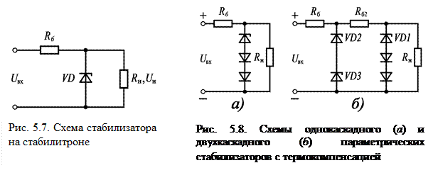
A schematic diagram of a parametric voltage stabilizer on a VD zener diode is shown in fig. 5.7. Ballast resistor resistance R b is selected so that the voltage drop across it is (0.5 ... 3) U n.
With an increase in voltage at the input of the stabilizer U input voltage at its output U out, i.e. on load R n tends to increase. But a slight increase in voltage D U st on a zener diode VD causes a sharp increase in current through it. This increases the voltage drop across the ballast resistor. R b, and the voltage at the load R n changes slightly. Voltage increment at the input of the stabilizer D U input is distributed between the voltage change on the ballast resistor D U R b in zener diode D U st: D U in -D U R b + D U Art. Since the resistance of the ballast resistor R b much more than the resistance of the zener diode R d ( R b >> R e), then almost the entire change in the input voltage is allocated to the resistance of the zener diode R and the voltage on the load remains stable.
The efficiency of such a zener diode does not exceed 30%, and the stabilization coefficient To st =50. To obtain a greater stabilization coefficient, a cascade connection of zener diodes is used, but at the same time, the efficiency of the stabilizer decreases sharply. To obtain a voltage greater than the parameters of one zener diode allow, they are connected in series (Fig. 5.8, b).
With an increase in ambient temperature for silicon zener diodes, the reverse voltage drop increases, and the forward voltage drop decreases. Therefore, silicon zener diodes connected in the reverse direction have a positive temperature coefficient of voltage TKV, and the same zener diodes connected in the forward direction have a negative TKV. For thermal compensation, a diode with a negative TKN is connected in series with the zener diode, or a zener diode in the forward direction, which has a negative TKN (Fig. 5.8). To fully compensate for the positive TKN of one zener diode, it is necessary to turn on several zener diodes in the forward direction, which have a negative TKN.
Parametric DC voltage stabilizers on silicon zener diodes have the following disadvantages:
small allowable power in the load (0.5 ... 3 W),
low stabilization coefficient (up to 30);
high output impedance of the stabilizer (6 ... 20 ohms);
dependence of zener diode parameters on temperature;
low efficiency (up to 30%).
Due to these shortcomings, parametric stabilizers based on silicon zener diodes are used to stabilize the supply voltage of auxiliary communication equipment nodes, where high quality indicators are not required.
Advantages: simplicity of the scheme, small dimensions and weight.
Parametric stabilizers based on silicon zener diodes are widely used in compensating voltage stabilizers as reference voltage sources.
In a two-stage parametric stabilizer, the circuit of which is shown in fig. 5.8, b, an output stage consisting of a zener diode VD 1 and quenching resistor R b2, powered by a preliminary stabilizer made on zener diodes VD 2, VD 3, and resistor R b1. The stabilization coefficient of such a circuit is equal to the product of the stabilization coefficients of the individual stages.
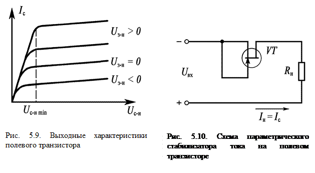
Parametric DC stabilizers is carried out on nonlinear elements, the current of which depends little on the voltage applied to them. As such an element, a field-effect transistor or a depleted-type MOSFET is used. From the characteristics of these transistors, shown in fig. 5.9, it can be seen that at a constant gate-source voltage, the drain current changes slightly with a change in the drain-source voltage.
On fig. 5.10 shows a diagram of a parametric DC stabilizer on a field-effect transistor with a shorted gate-source participation. Transistor in series with load resistance R n.
The disadvantage of this circuit is the inability to accurately set the value of the stabilized current due to the spread of the parameters of field-effect transistors. But by including an automatic bias resistor in the source circuit (Fig. 5.11), you can build an adjustable current stabilizer.
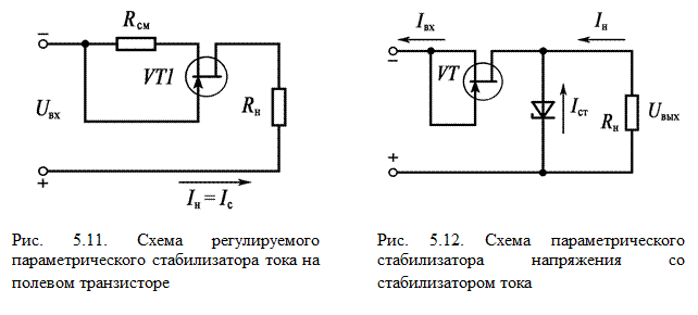
Current stabilizers are used in parametric DC voltage stabilizers to stabilize the input current. It is included instead of quenching resistance (Fig. 5.12), which increases the stabilization coefficient. When the input voltage changes, the input current, the stabilizer current, and, consequently, the output voltage change slightly. The use of a transistor current regulator instead of a quenching resistor makes it possible to increase the efficiency of a parametric voltage regulator, since it operates at lower input voltage values.
5.5. COMPENSATION STABILIZERS
DC VOLTAGE WITH CONTINUOUS REGULATION
Compensation Voltage Stabilizers with Continuous Regulation are closed-loop control systems or deviation control systems. They are performed according to the block diagrams shown in Fig. 5.13.
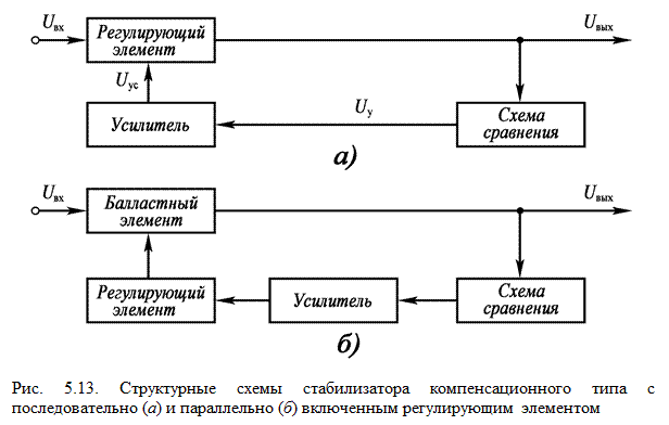
The output voltage is measured by the measuring element and compared with the reference voltage in the comparison circuit (CC). When the output voltage deviates from the set value, an error signal is generated at the SS output, which is amplified by the amplifier (U) and fed to the control element (RE). Under the influence of the mismatch signal, the internal resistance of the RE changes, and, consequently, the voltage drop across it. Changing the voltage on the RE compensates for the deviation of the output voltage U out of the set value with a certain degree of accuracy. Thus, at the end of the stabilization process, the output voltage will be stabilized:
U out = U in + U R e \u003d const.
Schematic diagram of a compensating DC voltage stabilizer with serial connection of RE and load R n is shown in fig. 5.14. The functions of the CC are performed by a bridge consisting of resistors R2, R3, R4 and zener diode VD1. Amplifier function - transistor VT2, RE function - transistor VT1. The reference voltage is the stabilization voltage of the zener diode VD1, which together with the resistor R2 forms a parametric constant voltage stabilizer. It is powered by the output voltage of the stabilizer, which is applied to the diagonal of the bridge ( ab). The emitter-base section of the transistor is connected to the other diagonal of the bridge VT2(amplifier input). Resistor R1 is the load in the collector circuit of the amplifier VT2.
Voltage stabilization U output on the load is carried out as follows. Assume that the voltage at the input of the stabilizer U vx decreased. Output voltage U the output of the stabilizer will first also decrease. As a result, the voltage drop across the resistor will decrease. R4 next divisor R3, R4. It's a voltage drop U2 compared with the reference voltage of the zener diode VD1 and goes to the base of the transistor VT2. Emitter potential VT2 remains unchanged, since it is determined by the reference voltage U op. Therefore, the positive potential of the base VT2 will decrease, which will cause a decrease in the collector current VT2, resulting in a decrease in the voltage drop across the resistor R1 and the base potential of the transistor VT1 regarding the collector. Potential difference between base and emitter VT1 became more. As a result, the resistance of the emitter-collector section of the regulating transistor will decrease VT1 and the voltage drop across it, and the voltage across the load R will recover approximately to the nominal value.
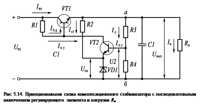
The circuit of the compensation stabilizer with the serial connection of the regulating transistor and the load has a high stabilization coefficient To st.n voltage and low output resistance only at low load current (no more than 10 mA). The reason for the low stabilization in this circuit is that in the regulating transistor VT1 as the input voltage changes, so does the base current I b.r., which leads to a decrease in the quality of stabilization.
To increase the voltage stabilization coefficient To st.n it is necessary that the collector current I k.u VT2 was much more than the base current I b2 ( I c.u. >> 10 I b.r.).
When this condition is met, the voltage drop across the resistor R1 determined mainly by the collector current of the amplifier VT2 I c.u., and the change in the base current I b.r will now depend on the voltage drop across the resistor R1. Condition fulfillment I c.u. >> 10 I b.r is achieved by using a composite control transistor and powering the amplifier from a separate stabilized power source.
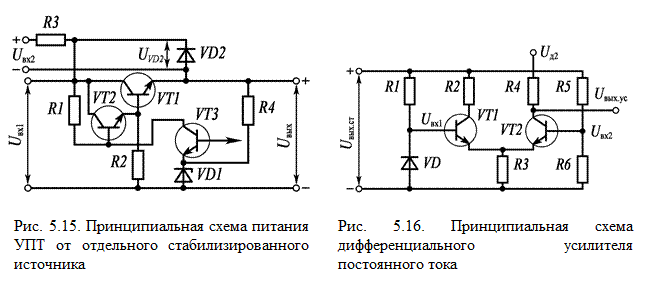
A schematic diagram of the power supply of the amplifier from a separate stabilized source is shown in fig. 5.15. Here is the amplifier power VT3 carried out by the sum of stabilized voltages U out + U VD2. Voltage U VD2, stabilized by a parametric stabilizer on VD2 and ballast resistor R3, obtained from a separate source U in2.
In the compensation DC voltage stabilizer, it is possible to adjust the output voltage U out. This is done by changing the resistance of the variable resistor R4. By changing the voltage at the base of the amplifying transistor, you can change its collector current I k.u., and consequently, the voltage drop from this current across the resistor R1, as a result of which the resistance of the emitter-collector junction of the regulating transistor changes. As a result, the stabilized voltage will change U out within certain limits.
To stabilize the parameters of the amplifier when the ambient temperature changes, a differential DC amplifier is used in the circuits of compensation stabilizers.
A schematic diagram of such an emitter-coupled amplifier is shown in fig. 5.16. The amplifier is connected to the output voltage of the stabilizer U vyh.st. For one entrance U input2 part of the voltage is supplied from the output of the stabilizer through the tracking divider R5, R6. To another amplifier input U input1 the reference voltage is supplied from the zener diode VD and resistor R1.
A change in ambient temperature causes a change in the collector currents of transistors VT1 and VT2. And since these transistors are connected by a common resistor in the emitter circuit R3, an increase in the collector current of one of the transistors causes a decrease
collector current of the other. As a result, the current through the resistor R3 and the output voltage of the amplifier U outputs change slightly. In a DC differential amplifier, the temperature drift of the emitter-base voltage of transistors is compensated VT1 and VT2.
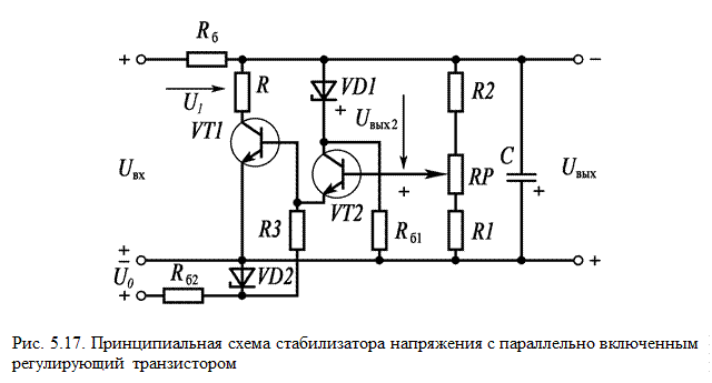
Schematic diagram of a semiconductor voltage regulator with a transistor connected in parallel is shown in fig. 5.17. It consists of a regulating transistor VT1, ballast resistor R b, amplifying element on a transistor VT2 and resistor R3, reference voltage source (ION) VD1 and R b1, voltage divider R1, RP, R2, additional source U 0 and R b2, VD2 to power the amplifying element of the circuit and the output capacitance FROM.
Voltage stabilization is carried out as follows. As the input voltage increases, the output voltage begins to increase. U out. The voltage drop across the resistor will also increase. R2 U out2 . The base potential will become more negative with respect to the emitter. Amplifying transistor collector current VT2 will increase. This will cause an increase in the voltage drop across the resistor. R3. As a result of this, the negative potential at the base of the regulating transistor will increase. VT1, which will increase the collector current I k1 and will cause growth total current scheme I 1 = I k1 + I n. And consequently, the voltage drop across the ballast resistor will increase R b, which will cause a decrease in the voltage at the output of the stabilizer to its original value. The output voltage is adjusted variable resistor RP.
The main advantages of stabilizers with RE parallel connection in comparison with stabilizers with RE connected in series: constant input current with changes in load resistance (at constant input voltage) and insensitivity to short circuits at the output.
Disadvantage: low efficiency.
Structural diagram of DC compensating stabilizer with serial connection of RE is shown in fig. 5.18. The voltage on the measuring element IE linearly depends on the change in the load current I n. The principle of operation of the scheme is as follows. When the load resistance changes R n load current starts to change I n what causes the change; voltage drop across the IE. The voltage on the IE is compared with the reference voltage, and their difference is fed to the input of the DC amplifier UPT, amplified and acts on the control element of the RE. 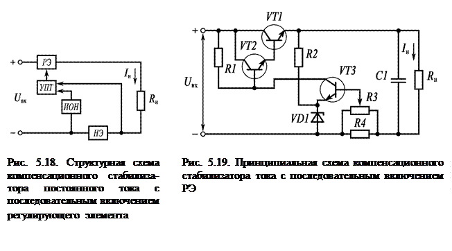 The resistance of the regulating element changes so that the deviation of the load current is compensated I n from the nominal value.
Schematic diagram of the compensation current stabilizer is shown in fig. 5.19. Here the function of the measuring element is performed by the resistor R4. Assume that the load resistance has decreased. Load current I n increased, the voltage drop across the resistor R4 also increased. As a result, the positive potential at the base of the amplifying transistor VT3 increases. Emitter potential VT3, determined by the reference voltage source on the stabilizer VD1, Will not change. Collector current VT3 and the voltage drop across the resistor R1 increase, lowering the potential of the base of the composite transistor of the regulating element VT1, VT2. The base current of the composite transistor decreases. Voltage drop across the emitter-collector junction of the transistor VT1 increases, decreasing the voltage across the load resistance R n. The resulting increase in current is compensated and maintained at a given level with a certain degree of accuracy. Stabilization of the current flowing through the changing load resistance is carried out by automatically changing the voltage applied to this resistance.
5.6. COMPENSATION STABILIZER
AC VOLTAGE
To stabilize the alternating voltage, ferromagnetic devices are used as a regulatory element, the resistance of which is alternating current varies depending on the DC current generated by the feedback circuit.
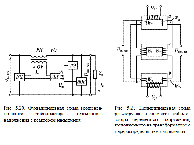
The simplest functional compensation voltage regulator circuit shown in fig. 5.20. Variable output voltage deviation U vyh.per from the nominal value is measured by the measuring element IE and compared with the reference voltage. The mismatch signal obtained as a result of the comparison is amplified by the DC amplifier UPT. Amplified current I y enters the control winding of the OS of the saturation reactor of the launch vehicle and changes the degree of magnetization of the magnetic circuit of the launch vehicle. This changes the resistance working winding RO to alternating current, and consequently, the voltage drop across it, which compensates for the deviation of the effective or amplitude output voltage from the nominal value. UPT is powered from a separate VSV rectifier.
Advantages of an AC voltage regulator with a saturation reactor:
high stabilization coefficient (several hundred);
high efficiency (0.9);
low sensitivity to changes in the frequency of the input voltage.
Flaws:
large weight and dimensions;
large response inertia: output voltage deviation is compensated in tens-hundreds of milliseconds after the deviation appears;
strong distortion of the shape of the curve of the output AC voltage, in which the third harmonic prevails;
big difference between input and output voltage.
Top performance The quality of AC voltage stabilization can be obtained by using transformers and autotransformers with voltage redistribution as a control element. In them, the power is divided into adjustable and unregulated. Stabilized in them is the voltage of only that part of the power flow, which is associated with a change in the input voltage U in. Therefore, the regulating element of such a stabilizer is performed at a low power, which is determined by the load current and the change in the input voltage U input
Voltage Sharing Transformer (TrPN) has three separate magnetic cores a, b, With(Fig. 5.21). On two magnetic circuits ( a and b) there are control windings W l a and W 1 b, designed to change the degree of bias depending on the constant voltages supplied to them U y a and U y b.
The main power flow is transmitted by a non-saturable transformer on a magnetic circuit With. Magnetic core transformers a and b designed to change voltage. The primary windings are connected in series and connected in parallel with the primary winding. W 1 transformer on the magnetic core With transmitting the main power flow. All secondary windings of transformers W 2 a, W 2 b and W 2 c interconnected in series. Moreover, the winding W 2a included opposite to the windings W 2 c and W 2 b.
The voltage at the output of such a device is equal to the geometric sum of the voltages taken from all secondary windings W 2 a, W 2 c:
U out = U 2a + W 2b + W 2c .
As the output voltage increases U output per winding voltage increase D U 2 a, D U 2 b, D U 2 c. To reduce the output voltage deviation D U you need to increase |D U 2 a| and decrease |D U 2 b|. And for this, the degree of magnetization of the magnetic circuit a must be reduced, and the magnetic circuit b- increase. This is done using a control scheme.
The same regulating element can be an autotransformer with voltage redistribution (ATrPN).
5.7. COMPENSATION STABILIZERS
ON MICROSCIRCUIT
At present, the industry produces integral compensation DC voltage stabilizers with continuous regulation of the K142EN series of three groups:
1. K142EN1; K142EN2; K142EN2A; KN2EN2B and K142ENZ; K142EN4 - with adjustable output voltage from 3 to 30 V.
2. K142EN5; K142EN5A; K142EN5B - with a fixed output voltage of 5 and 6 V.
4. K142EN6 - with bipolar adjustable output voltage from 5 to 15 V.
Advantages of integral DC voltage stabilizers of compensation type with continuous regulation:
high stabilization factor ( K st.n > 1000);
low output impedance ( R out. min £ 10 - 4 Ohm);
inertia of work;
high reliability;
no interference.
Flaws:
the need to use radiators that increase the size and weight;
low efficiency (0.4 ... 0.5).
Stabilizers K142EN1 and K142EN2 are most often used. In addition to their main purpose, they are used as active smoothing filters, current stabilizers, threshold devices, protection devices, etc.
On fig. 5.22 shows a diagram of an integrated compensation type stabilizer and one of the ways to turn it on. The regulating element of the stabilizer is made on a composite transistor VT4, VT3. The source of the reference voltage is a parametric stabilizer on a zener diode VD1. Reference voltage from zener diode VD1 enters the input of the emitter follower on the transistor VT5 and resistors R1, R2. With thermocompensating diode VD2 and resistor R2 to the input of the transistor VT6 constant voltage is applied. Transistor VT6 connected according to the scheme of the emitter follower, the load of which is the resistor R3. Resistor voltage R3 constant and equal to the voltage across the resistor R2. DC amplifier is made on transistors VT7 and VT2. Field-effect transistor VT2 is the collector load of the transistor VT7. Transistor VT2 has a large differential resistance, which increases the DC gain and reduces the effect of changes in the input voltage on the output.
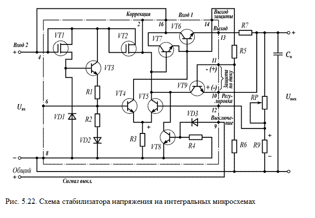
A transistor is included in the circuit to protect the stabilizer from short circuits and overloads. VT9. Turning off the stabilizer can be done using a transistor VT8. For the stabilizer to work, you need to connect a feedback divider to the circuit R8, R9, which has with the reference voltage source forms a control circuit. In addition, resistors of the protection circuit must be connected to the circuit. R5-R7 and output capacitor FROM.
The scheme works as follows. As the input voltage increases, the output voltage also increases. U out. Increased tension on the lower arm R9 U R 9 and hence the positive potential at the base of the transistor VT7 will increase. Its base and collector current will increase. The voltage drop across the load of the transistor will increase VT7, i.e. on the VT2, which will lead to a decrease in the currents of the base of the regulating element VT3, VT4, which close, and the collector-emitter voltage of the transistor VT4 increases. This leads to a decrease in the output voltage to its original value. The output voltage in the circuit is regulated by a variable resistor R8.
Protection of the stabilizer against short circuits and overloads is carried out by locking the composite control transistor. In normal mode and with small current overloads, the voltage across the resistor R7(current sensor) less voltage across the resistor R5. transistor based VT9- negative potential with respect to its emitter. Transistor VT9 closed. With significant overloads and short circuit resistor voltage R7 increases. And as soon as the voltage across the resistor R7 exceeds the voltage across the resistor R5, transistor base potential R9 becomes positive with respect to its emitter. Transistor VT9 opens, and its base and collector currents increase. Collector current rise VT9 leads to a decrease in the base currents of transistors VT3, VT4. They close, the current in the load circuit is limited.
Remote shutdown of the stabilizer is carried out by applying an external positive signal to the base of the transistor VT8. It opens, and the composite regulating transistor VT3, VT4 is locked. The voltage at the output of the stabilizer decreases to zero.
5.8. PULSE STABILIZERS
A voltage (current) stabilizer, the regulating element of which operates in the periodic switching mode, is called pulse regulated stabilizer or switching stabilizer (key).
Switching stabilizers are divided into:
according to the method of switching on the regulating element - into serial and parallel;
according to the method of control (regulation) - for stabilizers with pulse-width modulation - pulse-width (PWM); with pulse-frequency modulation - frequency-pulse (PFM);
relay or two-position.
Distinctive feature switching stabilizers is the high efficiency of the stabilizer as a whole (up to 0.9). This is a consequence of the pulsed mode of operation of the regulated element, in which the most significant part of the power lost on the elements of the stabilizer circuit is released. The regulating element in switching stabilizers is a periodically closing and opening transistor switch. In switching mode, the transistor is in saturation and cutoff modes most of the time. In these modes, the power released in the transistors is small, since either the voltage or the current of the transistor is very small. And the active switching mode is very fast. Therefore, the power lost on the regulating element is small.
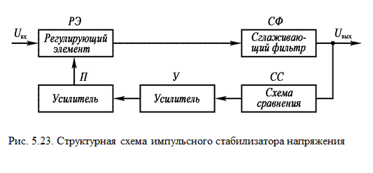
Operating principle switching regulator DC voltage is as follows. DC input voltage U input with the help of a regulating element is converted into a pulse and fed to the output, to the load, also in the form of pulses. Therefore, to obtain a constant voltage output in a switching regulator, a smoothing filter is needed. When the duration of the control pulses changes, the duration of the output voltage pulses changes accordingly, and, consequently, the average value of the voltage at the load also changes. If now a signal is introduced into the control circuit that is proportional to the deviation of the average voltage at the load from the specified one, then the output voltage will be stabilized in the circuit.
The block diagram of the switching voltage regulator is shown in fig. 5.23. The stabilizer includes: a regulating element RE, smoothing filter SF and a control circuit consisting of a comparison circuit SS, amplifier At and converter P. The comparison circuit and the amplifier are the same as in continuous compensation stabilizers. Pulse generators are used as a converter: multivibrators, triggers.
5.9. STABILIZERS
WITH TWO-POSITION REGULATION
In stabilizers with on-off regulation, both the frequency of the key and the duration of its closed state change. In this case, the control element switches from the closed state to the open state and vice versa when the output voltage reaches the threshold for actuation or release of the servo system that controls the operation of the control element.
Schematic diagram of a switching regulator of two-position (relay) voltage is shown in fig. 5.24. It includes the following elements: a regulating element on a composite transistor VT11, VT12, filter ( LC n, VD2), a comparison circuit and a DC amplifier ( R1, RP, R2, VD he, R G, VT y), tunnel diode flip-flop VD tg, transistor VT4 and resistor R8, intermediate amplifier ( VT3, R3, R4, R5). The locking of the regulating transistor is carried out using a transistor VT2. Elements R6, R zap, VD1, FROM zap provide reliable locking of the regulating transistor. Chain R9, C1 increases the frequency of self-oscillations of the stabilizer.
The principle of operation of the scheme is as follows. A constant voltage is applied to the input of the stabilizer U input Let us assume that the voltage at the output of the stabilizer has decreased to a value equal to the trigger voltage on VT4 and VD tg. trigger fired, transistor VT4 closes, and its collector current jumps to zero. current through resistor R5 does not leak, the positive potential of its base has decreased, and it closes. current through R3 no leakage, base potential VT2 rises and VT2 closes. transistors VT12 and VT11 open, condenser FROM Zap is charged through a resistor R6, voltage at the filter input in points BUT, B jumps up to voltage U input, diode VD2 closes, as the potential of its cathode becomes positive. Current through the regulating transistor VT11 and the inductor begins to increase, and the voltage at the output of the stabilizer decreases until it decreases to a value equal to the load current I n, after which it begins to grow.
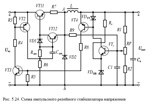
As the output voltage increases, the base potential VT y becomes more positive and its collector current increases. When the output voltage reaches the value U out + D U tg / a (where a is the transfer coefficient of the divider), collector current VT y reaches the trip current, the trigger fires, the transistor VT4 opens, and the current of its collector will increase abruptly to a maximum value. transistors VT3 and VT2 open. Capacitor FROM zap connects via VT2 to the base-emitter section of transistors VT12, VT11 and they close. At this time, the inductor is discharged through the diode VD2. While the inductor current L more load current, the voltage at the output of the stabilizer increases, and then begins to decrease. And at the same time, the positive voltage at the base of the amplifying transistor will decrease. VT y and its base and collector currents decrease. When the output voltage drops to the value U out - D U tg /a, collector current VT y will decrease to the value of the trigger release current. Trigger fired, transistors VT4, VT3, VT2 close, and the transistors VT12 and VT11 open. The collector current of the regulating transistor begins to increase again VT11, and hence the inductor current. In the future, the process is continuously repeated. As a result, the average value of the output voltage remains constant with a certain degree of accuracy.
Advantages of a relay-controlled stabilizer: simplicity of the circuit and relatively high speed.
Disadvantage: the presence of ripples at the output.
5.10. PULSE STABILIZERS
WITH PULSE-WIDTH CONTROL
The method of controlling the operation of the regulating transistor of a pulse stabilizer, in which a control signal with a constant repetition period and changing depending on the change in the output voltage with a pulse duration, is applied to the base, is called pulse-width. A device that converts a continuous signal into pulses of different durations is called a pulse-width modulator, and such a stabilizer is a pulse-width modulated stabilizer. In a pulse-width signal with a constant pulse repetition period T and = const fill factor changes K h = t n/ T n. There are two ways to change the duration of the pulses when the output voltage of the stabilizer deviates - the first and second kind.
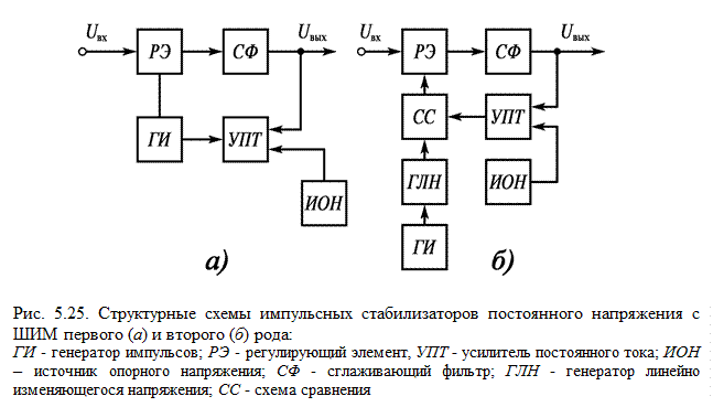
If the deviation of the output voltage of the stabilizer causes a change in the operating mode of the pulse generator (PG), at the output of which pulses of varying duration are formed, then this method of generating a pulse signal is called pulse-width modulation of the first kind. A block diagram of a switching DC voltage regulator with PWM of the first kind is shown in fig. 5.25, a.
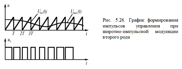
If the voltage at the output of the stabilizer U the output is compared with a linearly varying voltage U pl ( t) having a constant repetition period T(Fig. 5.26), and the duration of the pulses relative to constant values nt is determined by the moment of comparison of these voltages, then this method of generating a pulse signal is called pulse-width modulation of the second kind. The block diagram of such a stabilizer is shown in fig. 5.25, b.
The process of forming a pulse signal in a pulse-width modulator of the second kind is shown in fig. 5.26. Here, the upper graph shows sawtooth pulses with a linearly changing leading edge. U pl ( t). On the same graph, the curve U out ( t) depicts the changing voltage at the output of the stabilizer. The lower graph shows pulses whose width (duration) changes with the change in the output voltage of the stabilizer. The beginnings of the pulses of the upper and lower graphs coincide, and the ends are determined by the output voltage. As a result, pulses are obtained, the width of which is proportional to the deviations of the output voltage.
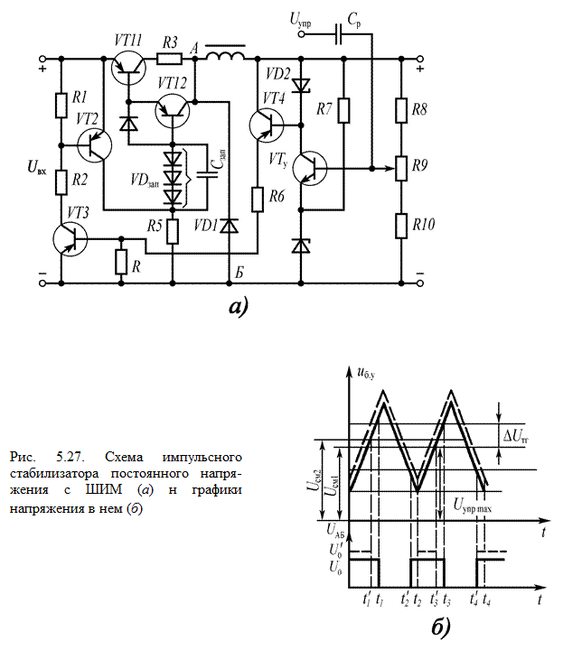
A schematic diagram of a PWM stabilizer is shown in fig. 5.27. It is slightly different from the relay stabilizer circuit (see Fig. 5.24). The input of the amplifier is sawtooth voltage U control and constant offset from the divider of the comparison circuit to R8, R9, R10. When the voltage at the base of the amplifying transistor reaches a value at which the collector current VT y will be equal to the trigger current ( VD2) (t 1 in fig. 5.27, b), a tunnel diode trigger, and VT4 work. transistors VT4, VT3 and VT2 open, a VT12 and VT11 are closed. Filter output voltage (points BUT, B) drops to zero. When the sawtooth voltage at the base of the transistor VT4 decrease ( t 2 in fig. 5.27, b) to a value at which the collector current of the amplifying transistor becomes equal to the release current of the trigger, the trigger will work, transistors VT4, VT3 and VT2 close, a VT12 and VT11 open. The voltage at the output of the filter will increase abruptly and become equal to the input voltage U input In the future, the trigger and the regulating transistor will continuously switch under the influence of an external alternating signal. With an increase in voltage at the input of the stabilizer, the open state of the transistors VT12 and VT11 decreases. Therefore, the duration of the pulse at the input of the filter decreases, and the average value of the output voltage returns to its original value with a certain degree of accuracy.
Scheme of a switching voltage stabilizer, in which the regulating element is made on a composite transistor VT11, VT12, VT13 shown in fig. 5.28. At the beginning of the circuit, the composite transistor is locked by a positive voltage from an external source E add. To the input of a differential transistor amplifier VT4, VT5 two voltages are supplied: part of the output voltage from the divider R4, RP, R6 and reference voltage from the zener diode VD4. They are compared. The mismatch signal is amplified and fed to a multivibrator on transistors VT7, VT8. Output voltage change U out causes a change in the duration of the pulses generated by the multivibrator and their duty cycle Q=T/t n, where t n is the duration of negative pulses. From the output of the multivibrator, a negative pulse is amplified in current by an emitter follower on a transistor VT6 and fed to the base of the transistor VT13, opening the composite transistor of the circuit for the duration of the multivibrator pulse. The voltage drop across the transistor changes and leads to the restoration of the output voltage to its previous value. Therefore, in 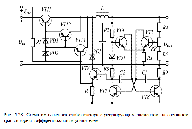 this scheme automatic regulation the output voltage is carried out due to negative feedback, as in continuous stabilizers.
5.11. SURGE PROTECTORS
ON THYRISTORS
On thyristors, voltage stabilizers can be made at a much higher power (up to 1000 V × A) with high efficiency - up to 95%. In addition, thyristors make it possible to combine the functions of rectification, regulation and stabilization, as well as to stabilize both direct and alternating voltages.
The functional diagram of the thyristor DC voltage stabilizer is shown in fig. 5.29. It contains a rectifier, the output voltage of which must be stabilized by the circuit. The principle of stabilization in this scheme is based on the change
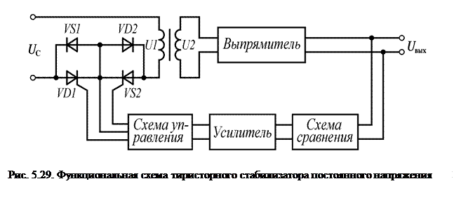
 the thyristor switching angle a t. The change in the output voltage of the stabilizer after the comparison circuit is fed to the amplifier, after which it is fed to the control circuit, where control pulses are formed. Their phase depends on the deviation of the output voltage. With an increase in the output voltage of the stabilizer U vx increases. This leads to a decrease in the operating time of the thyristor, and hence to a decrease in the current through the transformer Tr. The voltage at the output of the transformer will decrease and reduce the voltage at the output of the stabilizer U out to the previous value.
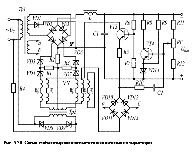
On fig. 5.30 shows a diagram of a stabilized thyristor power supply. The mains voltage is rectified by a bridge circuit on diodes VD2-VD5 and thyristors VS1, VS2. Thyristors are controlled by a differential magnetic amplifier MU, the voltage to which is supplied through the transformer Tr2. voltage stabilization primary winding carried out by zener diodes VD8 and VD9. This stabilization ensures the constancy of the thyristor current amplitude when the mains voltage changes. Control winding supply MU (W y) supplied by auxiliary bridge rectifier VD10-VD13. The control signal to this bridge circuit is supplied from the output of the second stage of the transistor amplifier VT3.
The circuit works as follows. The change in the output voltage after the comparison circuit and amplification of the control signal is fed into the winding W y differential magnetic amplifier. The changing current in the control winding causes a change in the switching angle of the thyristors a t, which leads the output voltage to the previous value.
TEST QUESTIONS
1 What is voltage stabilizer and current stabilizer?
2 Explain the purpose of voltage and current stabilizers.
3 What stabilizers are called parametric?
4 Draw a parametric diagram of a voltage regulator on a saturated core inductor and explain its operation.
5 Draw a diagram of a ferroresonant AC voltage regulator and explain how it works.
6 What are the advantages of ferroresonant stabilizers.
7 Draw the current-voltage characteristic of the silicon zener diode.
8 Explain the principle of the zener diode.
9 What are the features of a parametric stabilizer on a silicon zener diode.
10 Draw a diagram of a parametric DC stabilizer on a field-effect transistor and explain its operation.
11 What are DC compensation stabilizers?
12 List the main elements of the compensation stabilizer circuit.
13 Draw a diagram of a compensation stabilizer with a series connection of a regulating element.
14 Draw circuit diagram stabilizer using a composite transistor and explain its features.
15 Draw a diagram of a compensation DC voltage stabilizer with a parallel connection of a regulating element and explain the principle of its operation.
16 Draw a diagram of a compensation DC stabilizer with a series connection of a regulating element and explain its operation.
17 Draw a functional diagram of a compensating AC voltage regulator and explain the principle of its operation.
18 Explain the operation of the AC voltage regulator on a transformer with voltage redistribution.
19 Explain the features of the compensation stabilizer on the chip.
20 Explain the operation of a switching voltage regulator.
21 Draw block diagram switching voltage regulator and explain its operation.
22 Draw a schematic diagram of a two-position voltage regulator and explain its operation.
23 Explain the principle of operation of the stabilizer with pulse-width regulation.
24 What is the essence of the thyristor voltage stabilizer?
We advise you to read
 Psychological characteristics of children in adolescence
 Transferring a child to another school - the procedure and necessary documents Whether to transfer a child to another school
, diagnosis, treatment Treatment of urogenital chlamydia") Chlamydia urogenital - description, causes, symptoms (signs), diagnosis, treatment Treatment of urogenital chlamydia
Chlamydia urogenital - description, causes, symptoms (signs), diagnosis, treatment Treatment of urogenital chlamydia The benefits and significance of hydroamino acid threonine for the human body L threonine what