D iodine- the simplest device in the glorious family of semiconductor devices. If we take a semiconductor plate, for example, germanium, and introduce an acceptor impurity into its left half, and a donor impurity into its right, then on the one hand we get a semiconductor of type P, respectively, on the other, type N. In the middle of the crystal, we get the so-called P-N transition as shown in Figure 1.
The same figure shows the conditional graphic designation of the diode in the diagrams: the output of the cathode (negative electrode) is very similar to the "-" sign. It's easier to remember that way.
In total, in such a crystal there are two zones with different conductivity, from which two conclusions come out, therefore the resulting device is called diode because the prefix "di" means two.
In this case, the diode turned out to be semiconductor, but similar devices were known before: for example, in the era electronic tubes there was a tube diode called a kenotron. Now such diodes have gone down in history, although adherents of the “tube” sound believe that even the anode voltage rectifier in a tube amplifier should be a tube one!
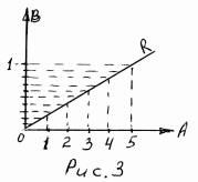
Figure 1. The structure of the diode and the designation of the diode in the diagram
At the junction of semiconductors with P and N conductivities, it turns out P-N junction (P-N junction), which is the basis of all semiconductor devices. But unlike a diode, which has only one junction, they have two P-N junctions, and, for example, they consist of four junctions at once.
P-N junction at rest
Even if the P-N junction, in this case the diode, is not connected anywhere, interesting physical processes still occur inside it, which are shown in Figure 2.
Figure 2. Diode at rest
In the N region there is an excess of electrons, it carries a negative charge, and in the P region the charge is positive. Together these charges form electric field. Since unlike charges tend to attract, electrons from the N zone penetrate into the positively charged P zone, filling some holes. As a result of such a movement inside the semiconductor, a current, although very small (units of nanoamperes), still arises.
As a result of such a motion, the density of matter on the P side increases, but up to a certain limit. Particles usually tend to spread evenly throughout the volume of a substance, just as the smell of perfume spreads throughout a room (diffusion), so, sooner or later, the electrons return back to the N zone.
If for most consumers of electricity the direction of the current does not play a role - the light bulb glows, the tile heats up, then for the diode the direction of the current plays a huge role. The main function of a diode is to conduct current in one direction. It is this property that is provided by the P-N junction.
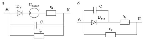
Turning on the diode in the opposite direction
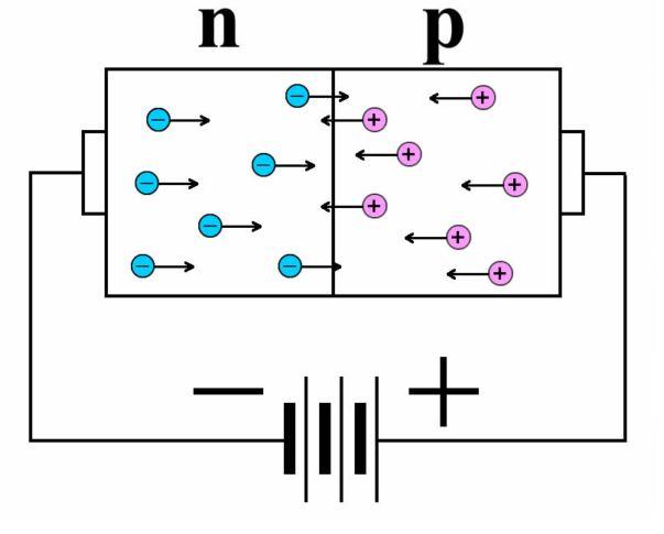
If you connect a power source to a semiconductor diode, as shown in Figure 3, then no current will pass through the P-N junction.
Figure 3. Diode reversed
As you can see in the figure, the positive pole of the power supply is connected to the N area, and the negative pole is connected to the P area. As a result, electrons from the region N rush to the positive pole of the source. In turn, positive charges (holes) in the P region are attracted by the negative pole of the power source. Therefore, in P-N areas transition, as can be seen in the figure, a void is formed, there is simply nothing to conduct current, there are no charge carriers.
As the power supply voltage increases, electrons and holes are attracted more and more. electric field batteries, in the region of the P-N junction, there are less and less charge carriers. Therefore, in the reverse connection, no current flows through the diode. In such cases, it is customary to say that semiconductor diode is locked by reverse voltage.
An increase in the density of matter near the poles of the battery leads to diffusion, - the desire for a uniform distribution of the substance throughout the volume. What happens when the battery is turned off.
Reverse current semiconductor diode
It is here that the time has come to recall the minor carriers that were conditionally forgotten. The fact is that even in the closed state, a small current passes through the diode, called reverse. This reverse current and is created by non-primary carriers, which can move in exactly the same way as the primary ones, only in the opposite direction. Naturally, such a movement occurs with a reverse voltage. The reverse current is usually small, due to the small number of minority carriers.
With an increase in the temperature of the crystal, the number of minority carriers increases, which leads to an increase in the reverse current, which can lead to P-N destruction transition. Therefore, operating temperatures for semiconductor devices - diodes, transistors, microcircuits are limited. To prevent overheating, powerful diodes and transistors are installed on heat sinks - radiators.
Turning on the diode in the forward direction
Shown in figure 4.
Figure 4. Diode direct connection
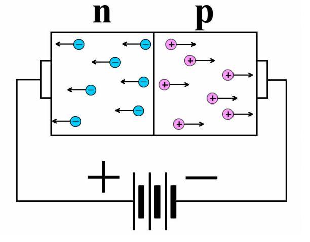
Now let's change the polarity of the source: connect the minus to the N region (cathode), and the plus to the P region (anode). With this inclusion in the N region, the electrons will be repelled from the minus of the battery, and move to P-N side transition. In the P region, positively charged holes will be repelled from the positive terminal of the battery. Electrons and holes rush towards each other.
Charged particles with different polarity gather near the P-N junction, an electric field arises between them. Therefore, the electrons overcome the P-N junction and continue to move through the P zone. At the same time, some of them recombine with holes, but most of them rush to the plus of the battery, the current Id went through the diode.
This current is called direct current. It is limited by the technical data of the diode, some maximum value. If this value is exceeded, then there is a danger of diode failure. However, it should be noted that the direction of the direct current in the figure coincides with the generally accepted, reverse movement of electrons.
It can also be said that in the direct direction of switching on electrical resistance diode is relatively small. When switched back on, this resistance will be many times greater, no current flows through the semiconductor diode (a slight reverse current is not taken into account here). From the foregoing, we can conclude that the diode behaves like a conventional mechanical valve: turned in one direction - the water flows, turned in the other - the flow has stopped. For this property, the diode was named semiconductor valve.
To understand in detail all the abilities and properties of a semiconductor diode, you should get acquainted with its volt - ampere characteristic. It's also a good idea to learn about the various diode designs and frequency properties, and the pros and cons. This will be discussed in the next article.
There is another way to reduce the voltage on the load, but only for DC circuits. See about here.
Instead of an additional resistor, a chain of diodes connected in series in the forward direction is used.
The whole point is that when current flows through the diode, a “forward voltage” drops on it, equal, depending on the type of diode, the power and current flowing through it, from 0.5 to 1.2 Volts.
On the germanium diode, the voltage drops 0.5 - 0.7 V, on the silicon diode from 0.6 to 1.2 Volts. Based on how many volts you need to lower the voltage at the load, turn on the appropriate number of diodes.
To lower the voltage by 6 V, you must approximately turn on: 6 V: 1.0 \u003d 6 pieces of silicon diodes, 6 V: 0.6 \u003d 10 pieces of germanium diodes. Silicon diodes are the most popular and available.
The above circuit with diodes is more cumbersome in execution than with a simple resistor. But, the output voltage, in a circuit with diodes, is more stable and weakly dependent on the load. What is the difference between these two methods of reducing the output voltage?
In Fig 1 - additional resistance - resistor (wire resistance), Fig 2 - additional resistance - diode.
A resistor (wire resistance) has a linear relationship between the current passing through it and the voltage drop across it. By how many times the current increases, the voltage drop across the resistor will increase by the same amount.
From example 1: if we connect another one in parallel to the light bulb, then the current in the circuit will increase, taking into account the total resistance of the two light bulbs up to 0.66 A. The voltage drop across the additional resistor will be: 12 Ohm * 0.66 A = 7.92 V The bulbs will remain: 12 V - 7.92 V = 4.08 V. They will burn to the floor of the glow.
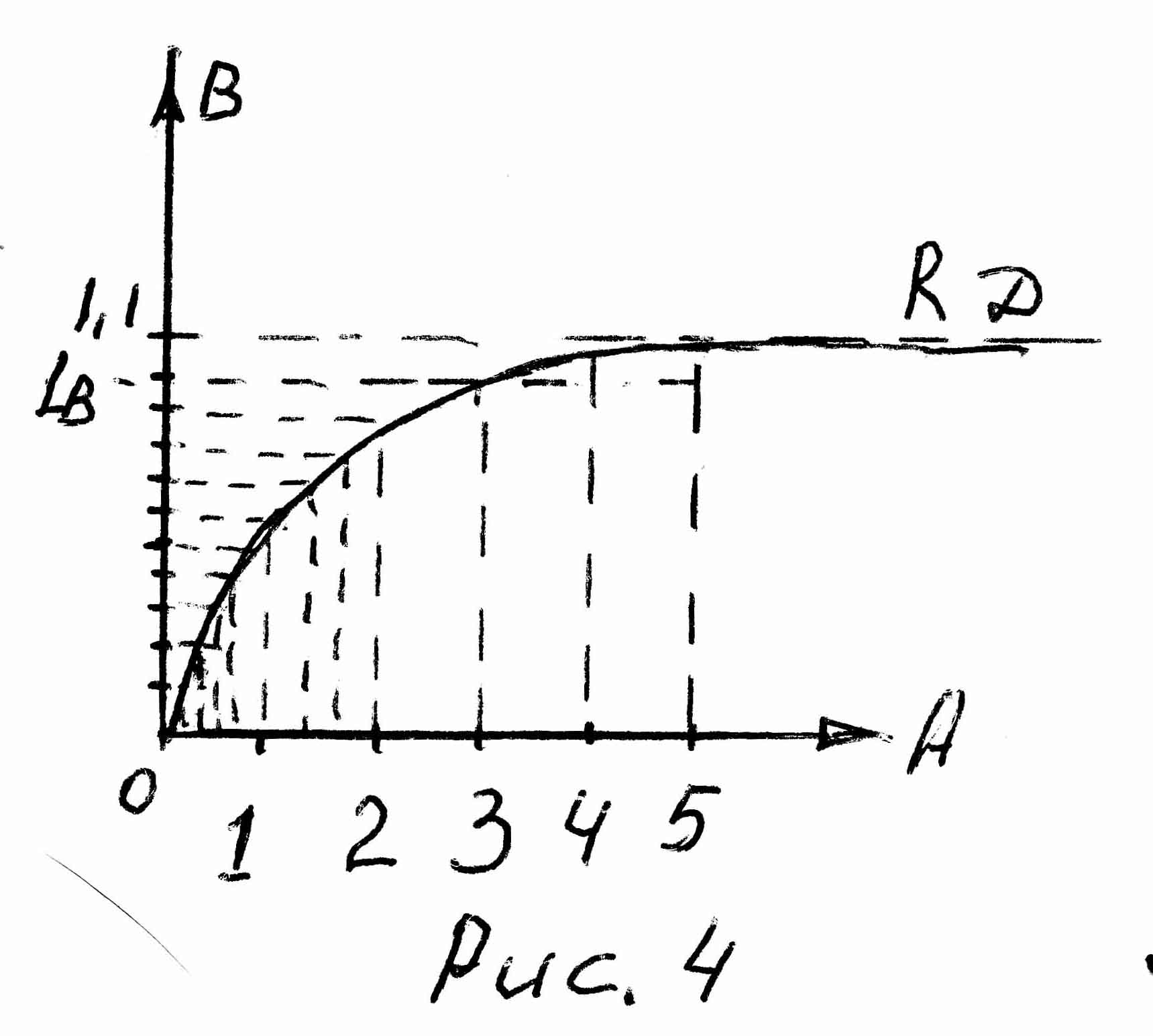
A completely different picture will be if instead of a resistor there is a chain of diodes.
The relationship between the current flowing through a diode and the voltage drop across it is non-linear. The current can increase several times, the voltage drop across the diode will increase by only a few tenths of a volt.
Those. the greater the current of the diode, the less (compared with the resistor) its resistance increases. The voltage drop across the diodes is little dependent on the current in the circuit.
Diodes in such a circuit act as a voltage stabilizer. Diodes must be selected according to the maximum current in the circuit. Maximum admissible current diodes must be greater than the current in the calculated circuit.
The voltage drops on some diodes at a current of 0.5 A are given in the table. 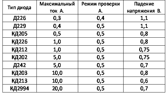
In chains alternating current, as an additional resistance, you can use a capacitor, inductance, dinistor or thyristor (with the addition of a control circuit).
Semiconductor diode - element electrical circuit, which has two terminals and has one-sided electrical conductivity. All semiconductor diodes can be divided into two groups: rectifier and special. Rectifier diodes, as the name suggests, are designed to rectify alternating current. Depending on the frequency and shape AC voltage they are divided into high-frequency, low-frequency and pulse. Special types of semiconductor diodes use different properties pn transitions: breakdown phenomenon, barrier capacitance, the presence of sections with negative resistance, etc.
Structurally, rectifier diodes are divided into planar and point, and according to manufacturing technology, into alloy, diffusion and epitaxial. Planar diodes due to large area pn-junctions are used to rectify high currents. Point diodes have a small junction area and, accordingly, are designed to rectify small currents. To increase the avalanche breakdown voltage, rectifier poles are used, consisting of a series of series-connected diodes.
High power rectifier diodes are called power diodes. The material for such diodes is usually silicon or gallium arsenide. Germanium is practically not used due to the strong temperature dependence of the reverse current. Silicon alloy diodes are used to rectify alternating current up to 5 kHz. Silicon diffusion diodes can operate at elevated frequencies up to 100 kHz. Silicon epitaxial diodes with a metal substrate (with a Schottky barrier) can be used at frequencies up to 500 kHz. Gallium arsenide diodes are capable of operating in the frequency range up to several MHz.
The operation of diodes is based on the use of an electron-hole junction - a thin layer of material between two areas different type electrical conductivity - n and p. The main property of this transition is asymmetric electrical conductivity, in which the crystal passes current in one direction and does not pass in the other. The device of the electron-hole transition is shown in Fig. 1.1, a. One part of it is doped with a donor impurity and has electronic conductivity ( n-region); the other, doped with an acceptor impurity, has hole conductivity ( p-region). The carrier concentrations in the regions differ sharply. In addition, both parts contain a small concentration of minority carriers.
Fig.1.1. pn transition:
a - device, b - space charges
Electrons in n- areas tend to penetrate into p- region where the electron concentration is much lower. Likewise, holes in p-areas are moved to n-region. As a result of the oncoming movement of opposite charges, a so-called diffusion current arises. Electrons and holes, having passed through the interface, leave behind opposite charges, which prevent the further passage of the diffusion current. As a result, dynamic equilibrium is established at the boundary, and when closing p- and n- areas no current flows in the circuit. The distribution of the space charge density in the transition is shown in Fig. 1.1, b. In this case, inside the crystal at the interface there is an own electric field E oct. , the direction of which is shown in Fig. 1.1, a. Its intensity is maximum at the interface, where there is an abrupt change in the sign of the space charge. And then the semiconductor is neutral.
Potential barrier height at pn transition is determined by the contact potential difference n- and p-areas, which, in turn, depends on the concentration of impurities in them:
![]() , (1.1)
, (1.1)
where is the thermal potential, N n and Pp are the concentrations of electrons and holes in n- and p-areas, n i is the concentration of charge carriers in the undoped semiconductor.
The contact potential difference for germanium is 0.6 ... 0.7 V, and for silicon - 0.9 ... 1.2 V. The height of the potential barrier can be changed by applying an external voltage to pn transition. If the field of the external voltage coincides with the internal one, then the height of the potential barrier increases; when the applied voltage is reversed, the barrier height decreases. If the applied voltage is equal to the contact potential difference, then the potential barrier disappears completely.
Hence, if an external voltage lowers the potential barrier, it is called direct, and if it increases it, it is called reverse.
The symbol and current-voltage characteristic (CVC) of an ideal diode are shown in Fig. 1.2.
The output to which a positive potential must be applied is called the anode, the output with a negative potential is called the cathode (Fig. 1.2, a). An ideal diode in the conductive direction has zero resistance. In the non-conductive direction - an infinitely large resistance (Fig. 1.2, b).
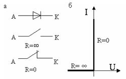
Fig. 1.2. Symbol (a) and CVC
characteristic of an ideal diode (b)
in semiconductors R-type, holes are the main carriers. Hole electrical conductivity was created by introducing atoms of an acceptor impurity. Their valency is one less than that of semiconductor atoms. In this case, impurity atoms capture semiconductor electrons and create holes - mobile charge carriers.
in semiconductors n-type the main carriers are electrons. Electronic electrical conductivity is created by introducing donor impurity atoms. Their valency is one more than that of semiconductor atoms. Forming covalent bonds with semiconductor atoms, impurity atoms do not use 1 electron, which becomes free. The atoms themselves become immobile positive ions.
If a voltage source is connected to the external terminals of the diode in the forward direction, then this voltage source will create in district transition electric field directed towards the internal. The resulting field will decrease. This will start the diffusion process. A direct current will flow in the diode circuit. The greater the value of the external voltage, the smaller the value of the internal field, the narrower the blocking layer, the greater the value of the forward current. With an increase in external voltage, the direct current increases exponentially (Fig. 1.3). When a certain value of the external stress is reached, the width of the barrier layer will decrease to zero. The forward current will be limited only by the volume resistance and will increase linearly as the voltage increases.
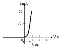
Fig.1.3. IV characteristic of a real diode
In this case, the voltage drop across the diode is a forward voltage drop. Its value is small and depends on the material:
germanium Ge: U pr= (0.3 - 0.4) V;
silicon Si: U pr\u003d (0.6 - 1) V.
If you change the polarity of the external voltage, then the electric field of this source will coincide with the internal one. The resulting field will increase, the width of the barrier layer will increase, and the current will ideally not flow in the opposite direction; but since semiconductors are not ideal and in addition to the main mobile carriers there are a small number of minor ones, as a result, a reverse current arises. Its value depends on the concentration of minority carriers and is usually a few to tens of microamperes.
The concentration of minority carriers is less than the concentration of major ones, so the reverse current is small. The magnitude of this current does not depend on the magnitude of the reverse voltage. Silicon reverse current is several orders of magnitude less than that of germanium, but silicon diodes have a higher forward voltage drop. The concentration of minority carriers depends on the temperature, and as it increases, the reverse current increases, so it is called the thermal current I o:
I o (T) \u003d I o (T o)e a D T,
DT=T-T o ; and Ge =0.09k -1; and Si \u003d 0.13k -1; I oGe >>I oSi . .
There is an approximate formula
I o (T)=I o (T o)2 T * ,
where T *- temperature increment, which corresponds to a doubling of the thermal current,
T*Ge=8...10 o C; T*Si=6°C.
Analytical expression for VAC r-p transition looks like:
 ,
(1.2)
,
(1.2)
where U is the applied external voltage.
For a temperature of 20 ° C φ t = 0.025V.
With an increase in temperature due to an increase in the thermal current and a decrease in the potential barrier, a decrease in the resistance of the semiconductor layers, a shift of the direct branch of the I–V characteristic occurs in the region of high currents. The volume resistance of semiconductors decreases n and R. As a result, the forward voltage drop will be less. As the temperature rises, the potential barrier of the barrier layer decreases due to a decrease in the difference between the concentrations of major and minor carriers, which will also lead to a decrease in U pr, since the barrier layer will disappear at a lower voltage.
The same current will correspond to different forward voltages (Fig. 1.4), forming the difference DU,
where e- temperature coefficient of voltage.
If the current through the diode is constant, then the voltage drop across the diode will decrease. With an increase in temperature by one degree, the forward voltage drop decreases by 2 mV.

Rice. 1.4. VAC r-p transition at Fig. 1.5. CVC of germanium and
different temperatures of silicon diodes
As the temperature rises, the reverse branch of the current-voltage characteristic shifts down (Fig. 1.4). The operating temperature range for germanium diodes is 80 ° C, for silicon diodes 150 ° C.
IV characteristics of germanium and silicon diodes are shown in Fig. 1.5.
Differential resistance r-p transition (Fig. 1.6):

 (1.3)
(1.3)
With increasing current r d- decreases.

Fig. 1.6. Definition of differential
diode resistance
Resistance direct current r-p transition: .
DC resistance is characterized by the slope of the straight line drawn from the origin to given point. This resistance also depends on the magnitude of the current: with increasing I, the resistance decreases . R Ge< R Si .
The IV characteristic of a semiconductor diode is somewhat different from the IV characteristic of an ideal diode. So, due to current leakage across the crystal surface, the real reverse current will be greater than the thermal current. Accordingly, the reverse resistance of a real diode is less than that of an ideal one. r-p transition.
Forward voltage drop is greater than ideal r-p transition. This is due to the voltage drop across the semiconductor layers. R and P type. Moreover, in real diodes one of the layers R or P has a higher concentration of major carriers than the other. A layer with a high concentration of majority carriers is called an emitter; it has negligible resistance. A layer with a lower concentration of majority carriers is called a base. It has quite a lot of resistance.
The increase in the forward voltage drop occurs due to the voltage drop across the base resistance.
For calculation electronic circuits containing semiconductor diodes, it becomes necessary to represent them in the form of equivalent circuits. The equivalent circuit of a semiconductor diode with a piecewise linear approximation of its CVC is shown in Fig. 1.7. Figure 1.8 shows equivalent circuits using the I–V characteristics of an ideal diode and the I–V characteristics of an ideal pn transition ( r d is the resistance of the diode, r is the leakage resistance of the diode).

Fig.1.7. Approximation of the current-voltage characteristic of a diode
linear segments
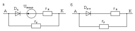
Fig.1.8. Replacing Diodes Using I-V Characteristics
ideal diode (a) and CVC ideal pn transition (b)
The operation of a diode in a circuit with a load. Consider the simplest circuit with a diode and a resistor, and the action of a bipolar voltage at its input (Fig. 1.9). The picture of the distribution of voltages on the circuit elements is determined by the position of the load lines (Fig. 1.10) - on the graph of the CVC of the diode along the voltage axis, two points are plotted in both directions, determined by +U m and –U m supply voltage, which corresponds to the voltage across the diode with a shorted load R n, and currents are deposited on the current axis in both directions U m / R n and - U m / R n, which corresponds to a shorted diode. These two points are connected in pairs by straight lines, which are called load. Load line intersections R n in the first and third quadrants with branches
I–V characteristics of the diode for each phase of the supply voltage correspond to
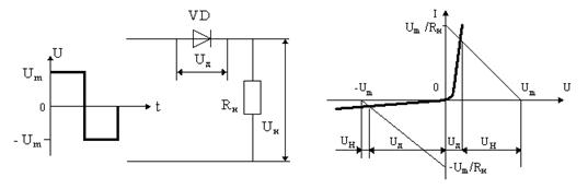
Rice. 1.9. Circuit with diode and Fig. 1.10. CVC diode with load
direct load
their identical currents (which is necessary when they are connected in series) and determine the position of the operating points.
positive half wave U>0, U=Um.
This polarity is direct for a diode. Current and voltage will always satisfy the current-voltage characteristic:
 ,
,
Moreover:
U d \u003d U m - I d R H;
at I d \u003d 0, U d \u003d U m;
at U d \u003d 0, I d \u003d U m / R H;
with direct connection U m >> U pr(Fig. 1.10).
At practical application U pr>0 (U pr- forward voltage) when the diode is open. When the diode operates in the forward direction, the voltage across it is minimal - ( Ge-0.4V; Si-0.7 V), and it can be considered approximately equal to zero. The current will then be maximum.

Fig.1.11. Voltage and current signals in a diode circuit with a load
 .
.
negative half wave U<0, U= -U m .
The characteristic of the diode is the same, but
U d \u003d -U m -I d R H,;
I d \u003d 0, U d \u003d U m;
U d =0, I d =U m /R H ; U H<
Capacities r-p transition. When turned on r-p transition in the opposite direction, as well as at small forward voltages in the region r-p transition there is a double electric layer: in R areas - negative, in P areas - positive.
The accumulation of an uncompensated charge in this layer leads to the appearance of a capacitance r-p transition, which is called the barrier capacitance. It characterizes the change in the accumulated charge with a change in the external voltage according to Fig. 1.12. C b \u003d dQ / dU .
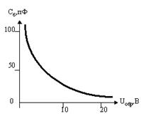
Rice. 1.12. Barrier capacitance dependence
from reverse voltage.
Barrier capacitance depends on geometric dimensions r-p transition. With the increase U arr width r-p transition increases, and the capacitance decreases.
When the diode is turned on in the forward direction, the barrier capacitance practically disappears, and the minority carriers transferred from the emitter accumulate in the base layer of the diode. This accumulation of charge also creates a capacitance effect, which is called diffusion capacitance. C d usually exceeds C b.
Diffusion capacity is determined C d \u003d dQ d / dU.
These capacitances affect the operation of diodes at high frequencies. Capacities r-p the transition is included in the equivalent circuit (Fig. 1.13).
Rice. 1.13. Diode equivalent circuits taking into account capacitances:
a – barrier capacitance; b - diffusion capacity
Transient processes in diodes. When diodes operate with high-frequency signals (1-10 MHz), the process of transition from a non-conductive state to a conductive state and vice versa does not occur instantly due to the presence of capacitance in the transition, due to the accumulation of charges in the diode base.
Figure 1.14 shows the timing diagrams of current changes through the diode and the load with rectangular pulses of the supply voltage. Capacitances in the diode circuit distort the leading and trailing edges of the pulses, causing the absorption time to appear tp.
When choosing a diode for a particular circuit, its frequency properties and speed must be taken into account.
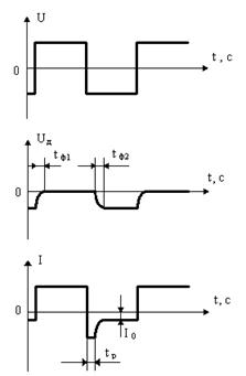
Rice. 1.14. Transient processes at
switching diode:
t f1- the duration of the leading edge of the transition;
t f2- the duration of the trailing edge;
tp- dissolution time.
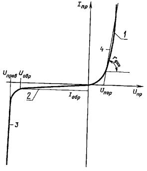
Breakdown r-p transition. The reverse voltage of the diode cannot increase to an arbitrarily large value. At some reverse voltage, characteristic of each type of diode, there is a sharp increase in the reverse current. This effect is called transition breakdown. There are several types of breakdown (Fig. 1.15):
1 - avalanche breakdown, when an increase in the reverse current occurs due to avalanche multiplication of non-main carriers;
Rice. 1.15. CVC for various types of breakdown
2-tunnel breakdown, when the overcoming of the potential barrier and the blocking layer occurs due to the tunnel effect.
During avalanche and tunnel breakdowns, the reverse current increases at a constant reverse voltage.
These are electrical breakdowns. They are reversible. After removal U arr the diode recovers its properties.
3- thermal breakdown, it occurs when the amount of heat released in r-p junction, more heat is given off by the surface of the diode to the environment. However, with increasing temperature r-p transition, the concentration of minority carriers increases, which leads to an even greater increase in the reverse current, which, in turn, leads to an increase in temperature, etc. Since for diodes made on the basis of germanium, I arr more than for silicon-based diodes, then for the former, the probability of thermal breakdown is higher than for the latter. Therefore, the maximum operating temperature for silicon diodes is higher (150 o ... 200 o C) than for germanium ones (75 o ... 90 o C).
With this breakdown r-p the transition is destroyed.
Test questions.
1. What is a semiconductor diode? Current-voltage characteristic of an ideal and real diode?
2. What materials are used to make semiconductor diodes? How to create regions of one or another type of conductivity in a semiconductor substrate?
3. What is the intrinsic electric field in a crystal at the boundary p-n- transition? How does it change when an external voltage is applied?
4. What explains the effect of one-way conduction p-n- junction in a semiconductor?
5. Current-voltage characteristics pn-transitions for germanium and silicon diodes when the external temperature changes?
6. How is the differential resistance of a diode determined?
7. How are the current-voltage characteristics of a diode with a load straight line constructed?
8. Explain the mechanism of formation of the barrier and diffusion capacitances of the diode? How do they affect the operation of the diode in AC circuits?
Lecture 2 Special types
Semiconductors are substances that occupy an intermediate position between conductors and insulators in their electrically conductive properties.
In semiconductors, as in metals, current is an ordered movement of charged particles.
However, along with the movement of negative charges (electrons) in semiconductors, there is an ordered movement of positive charges, the so-called. - holes.
holes obtained with the participation ions semiconductor substances - atoms with runaway electrons. In reality, ionized atoms do not leave their place in the crystal lattice. In fact, there is a gradual change in the state of the atoms of matter, when electrons jump from one atom to another. There is a process that outwardly looks like an ordered movement of some conditional positively charged particles - holes.
In an ordinary, pure semiconductor, the ratio holes and free electrodes 50%:50%.
But it is worth adding a small amount of substance - impurities to the semiconductor, as this ratio undergoes significant changes. Depending on the features of the added substance, the semiconductor acquires either a pronounced electronic conductivity (n-type), or holes (p-type) become its main carriers.
Semiconductor junction(p-n) is formed at the junction of two fragments of a semiconductor material having different conductivity. It is an extremely thin region depleted of both types of carriers. The p-n junction has little resistance when the direction of current is forward, and a very large resistance when the direction of current is reverse.
A conventional semiconductor diode consists of a single semiconductor junction provided with two terminals - anode(positive electrode) and cathode- negative electrode. Accordingly, the diode has the property unilateral conduction- it conducts current well in the forward direction and badly in the opposite direction.
What does this mean in practice?
Imagine an electrical circuit consisting of a battery and an incandescent light bulb connected in series through a semiconductor diode. The lamp will only light up if anode(positive electrode) is connected to the plus of the power source (battery) and cathode(negative electrode) to the minus - through the filament of the light bulb.
This is the direct inclusion of a semiconductor diode. If you reverse the polarity of the power supply, the diode will turn on in reverse - the light will not light. Pay attention to how the designation of a semiconductor diode looks on the diagram - a triangular arrow indicating direct connection coincides with the direction of current generally accepted in electrical engineering - from the plus of the power source to the minus. The vertical dash adjacent to it symbolizes an obstacle to the movement of current in the opposite direction.
There is one prerequisite for the normal operation of any semiconductor diode. The power supply voltage must exceed a certain threshold (the value of the internal bias potential p-n junction). For rectifier diodes, it is usually less than 1 volt, for germanium high-frequency diodes it is about 0.1 volts, for LEDs it can exceed 3 volts. This property of semiconductor diodes can be used to create low-voltage stabilized power supplies.
If you connect the diode back and gradually increase the voltage of the power source, at some point a reverse electrical breakdown of the p-n junction will definitely occur. The diode will begin to pass current in the opposite direction, and the junction will be damaged. The value of the maximum allowable reverse voltage (Ureverse) varies widely for different types of semiconductor diodes and is a very important parameter.
The second, no less important parameter can be called the limiting value of the forward current-Upr. This parameter directly depends on the magnitude of the voltage drop at the junction of the semiconductor diode, the material of the semiconductor and the heat transfer characteristics of the case.
The use of any materials on this page is allowed if there is a link to the site
It strongly depends on the concentration of impurities. Semiconductors whose electrophysical properties depend on impurities of other chemical elements are called impurity semiconductors. There are two types of impurities, donor and acceptor.
Donor an impurity is called, the atoms of which give the semiconductor free electrons, and the electrical conductivity obtained in this case, associated with the movement of free electrons, is electronic. A semiconductor with electronic conductivity is called an electronic semiconductor and is conventionally denoted by the Latin letter n - the first letter of the word "negative".
Let us consider the process of formation of electronic conductivity in a semiconductor. We take silicon as the main semiconductor material (silicon semiconductors are the most common). Silicon (Si) has four electrons in the outer orbit of the atom, which determine its electrophysical properties (that is, they move under the influence of voltage to create an electric current). When arsenic (As) impurity atoms are introduced into silicon, which has five electrons in the outer orbit, four electrons interact with four electrons of silicon, forming a covalent bond, and the fifth electron of arsenic remains free. Under these conditions, it easily separates from the atom and gets the opportunity to move in the substance.
acceptor An impurity is called an impurity whose atoms accept electrons from the atoms of the main semiconductor. The resulting electrical conductivity, associated with the movement of positive charges - holes, is called hole. A semiconductor with hole electrical conductivity is called a hole semiconductor and is conventionally denoted by the Latin letter p - the first letter of the word "positive".
Let us consider the process of formation of hole conductivity. when indium (In) impurity atoms are introduced into silicon, which has three electrons in the outer orbit, they bond with three electrons of silicon, but this bond turns out to be incomplete: one more electron is missing to bond with the fourth electron of silicon. The impurity atom attaches the missing electron from one of the nearby atoms of the main semiconductor, after which it becomes associated with all four neighboring atoms. Due to the addition of an electron, it acquires an excess negative charge, that is, it turns into a negative ion. At the same time, the semiconductor atom, from which the fourth electron left for the impurity atom, turns out to be connected with neighboring atoms by only three electrons. thus, there is an excess of positive charge and an unfilled bond appears, that is hole.
One of the important properties of a semiconductor is that in the presence of holes, a current can pass through it, even if there are no free electrons in it. This is due to the ability of holes to move from one semiconductor atom to another.
Moving "holes" in a semiconductor
By introducing a donor impurity into a part of a semiconductor and an acceptor impurity into another part, it is possible to obtain regions with electron and hole conductivity in it. A so-called electron-hole transition is formed at the boundary between the regions of electronic and hole conduction.
P-N junction
Consider the processes that occur when current passes through electron-hole transition. The left layer, labeled n, is electronically conductive. The current in it is associated with the movement of free electrons, which are conventionally indicated by circles with a minus sign. The right layer, denoted by the letter p, has hole conductivity. The current in this layer is associated with the movement of holes, which are indicated by circles with a “plus” in the figure.
Motion of electrons and holes in the direct conduction mode
Movement of electrons and holes in the reverse conduction regime.
When semiconductors with different types of conductivity come into contact, electrons due to diffusion will begin to move to the p-region, and holes - to the n-region, as a result of which the boundary layer of the n-region is charged positively, and the boundary layer of the p-region is negatively charged. An electric field arises between the regions, which is, as it were, barriers for the main current carriers, due to which a region with a reduced charge concentration is formed in the p-n junction. The electric field in the p-n junction is called a potential barrier, and the p-n junction is called a blocking layer. If the direction of the external electric field is opposite to the direction of the field of the p-n junction ("+" in the p-region, "-" in the n-region), then the potential barrier decreases, the concentration of charges in the p-n junction increases, the width and, therefore, the transition resistance decreases. When the polarity of the source is changed, the external electric field coincides with the direction of the field of the p-n junction, the width and resistance of the junction increases. Therefore, the p-n junction has valve properties.
semiconductor diode
diode called an electrically converting semiconductor device with one or more p-n junctions and two leads. Depending on the main purpose and the phenomenon used in the p-n junction, there are several main functional types of semiconductor diodes: rectifier, high-frequency, pulse, tunnel, zener diodes, varicaps.
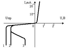
Basic characteristics of semiconductor diodes is the current-voltage characteristic (VAC). For each type of semiconductor diode, the I–V characteristic has a different form, but they are all based on the I–V characteristic of a junction rectifier diode, which has the form:
Current-voltage characteristic (CVC) of the diode: 1 - direct current-voltage characteristic; 2 - reverse current-voltage characteristic; 3 - breakdown area; 4 - rectilinear approximation of the direct current-voltage characteristic; Upor is the threshold voltage; rdyn is dynamic resistance; Uprob - breakdown voltage
The scale along the y-axis for negative values of currents is chosen many times larger than for positive ones.
The current-voltage characteristics of the diodes pass through zero, but a sufficiently noticeable current appears only when threshold voltage(U then), which for germanium diodes is 0.1 - 0.2 V, and for silicon diodes it is 0.5 - 0.6 V. In the region of negative voltage values on the diode, at already relatively low voltages (U arr. ) occurs reverse current(I arr). This current is created by minority carriers: electrons of the p-region and holes of the n-region, the transition of which from one region to another is facilitated by a potential barrier near the interface. With an increase in the reverse voltage, an increase in current does not occur, since the number of minority carriers that appear at the transition boundary per unit time does not depend on the voltage applied from outside, if it is not very large. The reverse current for silicon diodes is several orders of magnitude less than for germanium ones. Further increase in reverse voltage to breakdown voltage(U samples) leads to the fact that electrons from the valence band pass into the conduction band, there is zener effect. In this case, the reverse current increases sharply, which causes heating of the diode and a further increase in current leads to thermal breakdown and destruction of the p-n junction.
Designation and definition of the main electrical parameters of diodes
Semiconductor diode designation
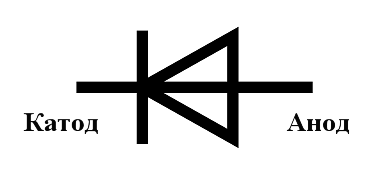
As mentioned earlier, the diode conducts current in one direction (i.e., ideally, it is just a conductor with low resistance), in the other direction it does not (i.e., it turns into a conductor with very high resistance), in a word, it has unilateral conduction. Accordingly, he has only two conclusions. They, as has been customary since the time of lamp technology, are called anode(positive conclusion) and cathode(negative).
All semiconductor diodes can be divided into two groups: rectifier and special. Rectifier Diodes, as the name implies, are designed to rectify alternating current. Depending on the frequency and shape of the alternating voltage, they are divided into high-frequency, low-frequency and pulse. Special types of semiconductor diodes use different properties p-n-transitions; breakdown phenomenon, barrier capacitance, the presence of areas with negative resistance, etc.
Rectifier Diodes
Structurally, rectifier diodes are divided into planar and point, and according to manufacturing technology, into alloy, diffusion and epitaxial. Planar diodes, due to the large area of the p-n junction, are used to rectify high currents. Point diodes have a small junction area and, accordingly, are designed for rectification small currents. To increase the avalanche breakdown voltage, rectifier poles are used, consisting of a series of diodes connected in series.
High power rectifier diodes are called power. The material for such diodes is usually silicon or gallium arsenide. Silicon alloy diodes are used to rectify alternating current with a frequency of up to 5 kHz. Silicon diffusion diodes can operate at higher frequencies, up to 100 kHz. Silicon epitaxial diodes with a metal substrate (with a Schottky barrier) can be used at frequencies up to 500 kHz. Gallium arsenide diodes are capable of operating in the frequency range up to several MHz.
Power diodes are usually characterized by a set of static and dynamic parameters. To static parameters diodes include:
- voltage drop U CR on the diode at a certain value of direct current;
- reverse current I arr at a certain value of the reverse voltage;
- mean direct current I pr.cf. ;
- impulsive reverse voltage U arr. ;
To dynamic parameters diode are its time and frequency characteristics. These options include:
- recovery time t reverse voltage;
- rise time direct current I out. ;
- limit frequency without reducing the modes of the diode f max .
Static parameters can be set according to the current-voltage characteristic of the diode.
The reverse recovery time of the diode tvos is the main parameter of rectifier diodes, which characterizes their inertial properties. It is determined by switching the diode from a given forward current I CR to a given reverse voltage U arr. During switching, the voltage across the diode acquires the opposite value. Due to the inertia of the diffusion process, the current in the diode does not stop instantly, but over time t nar. In essence, there is a resorption of charges at the boundary of the p-n junction (ie, a discharge of equivalent capacity). It follows from this that the power losses in the diode increase sharply when it is turned on, especially when it is turned off. Consequently, losses in the diode increase with increasing frequency of the rectified voltage.
When the temperature of the diode changes, its parameters change. The forward voltage on the diode and its reverse current depend most strongly on temperature. Approximately, we can assume that TKN (voltage temperature coefficient) Upr \u003d -2 mV / K, and the reverse current of the diode has a positive coefficient. So with an increase in temperature for every 10 ° C, the reverse current of germanium diodes increases by 2 times, and silicon - 2.5 times.
Diodes with a Schottky barrier
For rectification of small voltages of high frequency are widely used schottky barrier diodes. In these diodes, instead of a p-n junction, a metal surface contact with is used. At the point of contact, semiconductor layers depleted in charge carriers, which are called shut-off layers, appear. Diodes with a Schottky barrier differ from diodes with a p-n junction in the following ways:
- more low straight voltage drop;
- have more low reverse voltage;
- more high current leaks;
- almost no charge reverse recovery.
Two main characteristics make these diodes indispensable: low forward voltage drop and fast reverse voltage recovery time. In addition, the absence of minor media requiring recovery time means physical no loss to switch the diode itself.
The maximum voltage of modern Schottky diodes is about 1200 V. At this voltage, the forward voltage of the Schottky diode is less than the forward voltage of diodes with a p-n junction by 0.2 ... 0.3 V.
The advantages of the Schottky diode become especially noticeable when rectifying low voltages. For example, a 45-volt Schottky diode has a forward voltage of 0.4 ... 0.6 V, and at the same current, a p-n-junction diode has a voltage drop of 0.5 ... 1.0 V. When the reverse voltage drops to 15 V, the forward voltage decreases to 0.3 ... 0.4 V. On average, the use of Schottky diodes in the rectifier makes it possible to reduce losses by about 10 ... 15%. The maximum operating frequency of Schottky diodes exceeds 200 kHz.
Theory is good, but theory without practice is just shaking the air.
We advise you to read
 Psychological characteristics of children in adolescence
 Transferring a child to another school - the procedure and necessary documents Whether to transfer a child to another school
, diagnosis, treatment Treatment of urogenital chlamydia") Chlamydia urogenital - description, causes, symptoms (signs), diagnosis, treatment Treatment of urogenital chlamydia
Chlamydia urogenital - description, causes, symptoms (signs), diagnosis, treatment Treatment of urogenital chlamydia The benefits and significance of hydroamino acid threonine for the human body L threonine what