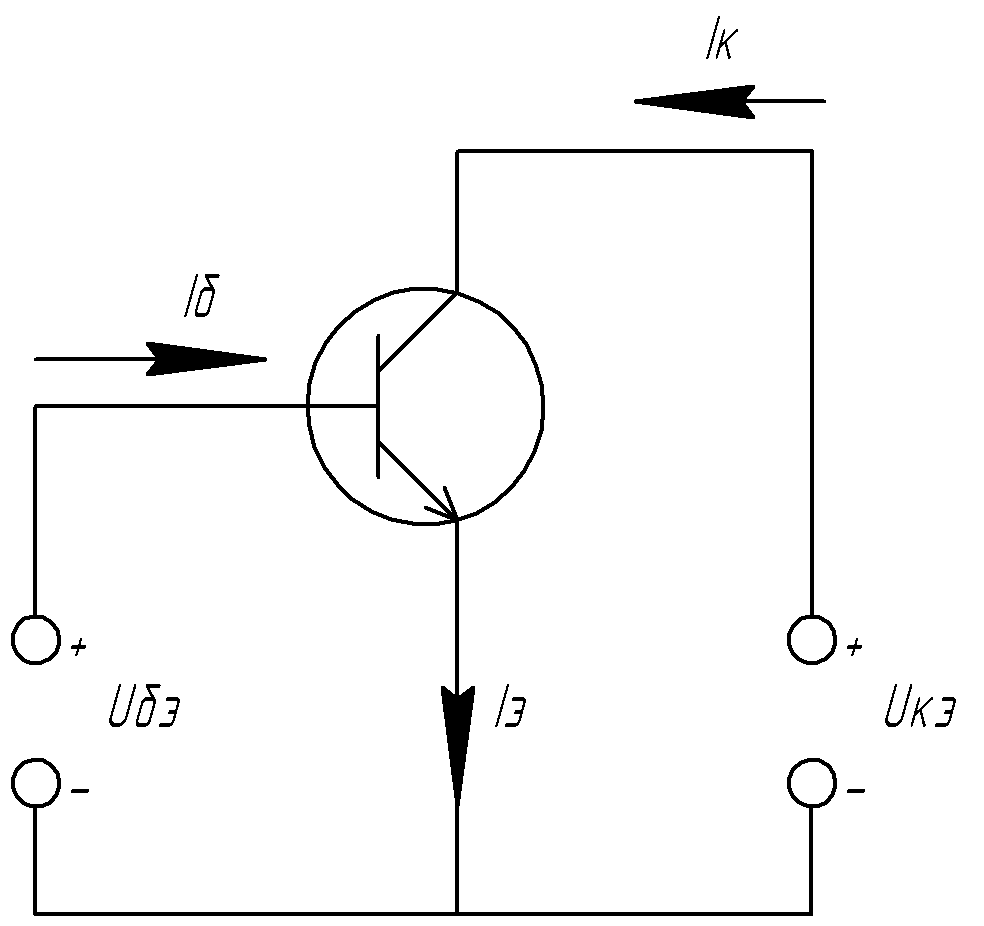
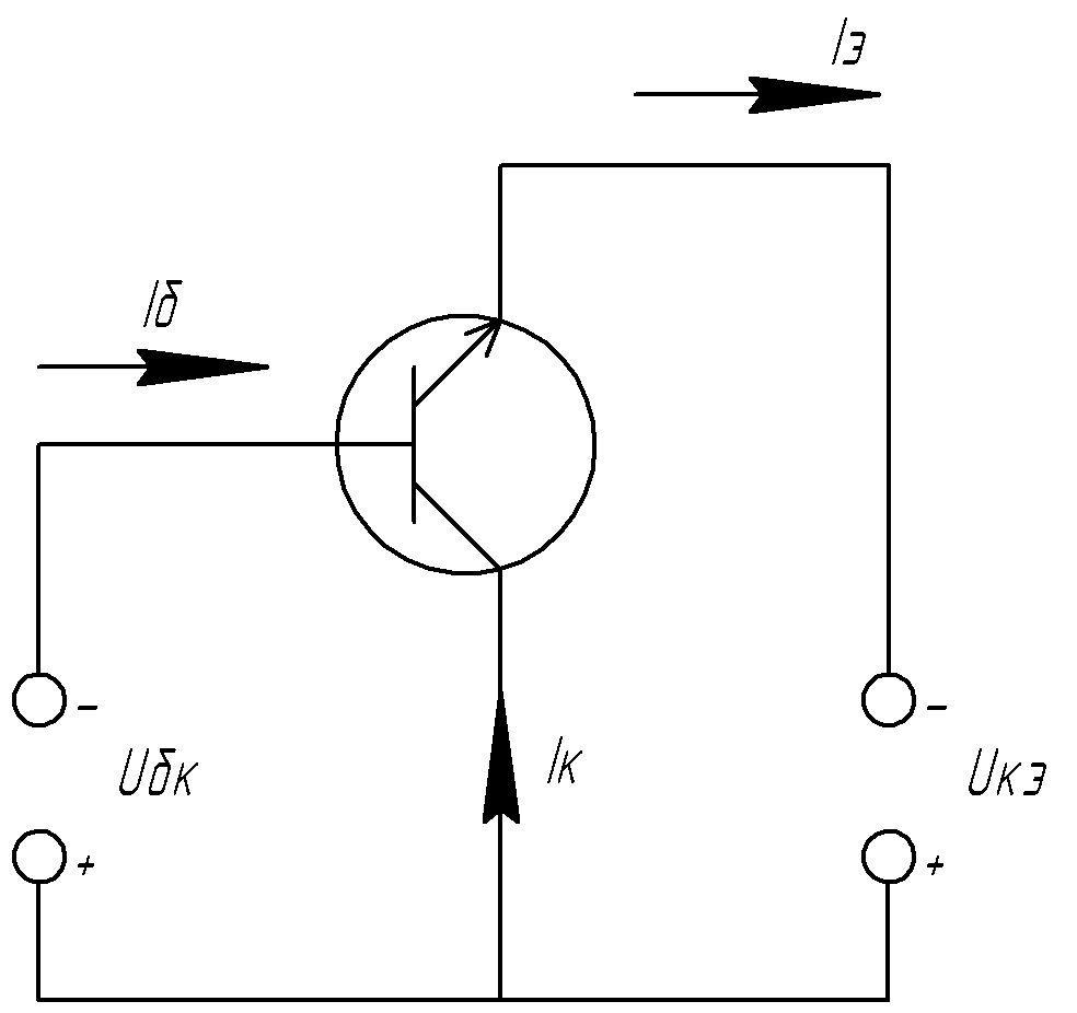
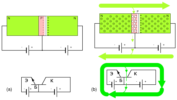
Designation of bipolar transistors on the diagrams
bipolar transistor- a three-electrode semiconductor device, one of the types of transistors. In the semiconductor structure, 2 p-n junction and charge transfer in the device is carried out by carriers of 2 types - electrons and holes. That is why the device was called "bipolar".
It is used in electronic devices to enhance the generation of electrical oscillations and as a current switching element, for example, in electronic logic circuits.
The electrodes are connected to three consecutive layers of a semiconductor with an alternating type of impurity conduction. According to this method of alternation, n-p-n and p-n-p transistors ( n (negative) - electronic type of impurity conductivity, p (positive) - hole).
The operation of a bipolar transistor, unlike a field effect transistor, is based on the transfer of two types of charges simultaneously, the carriers of which are electrons and holes (from the word "bi" - "two"). The schematic diagram of the transistor is shown in the second figure.
The electrode connected to the middle layer is called base, the electrodes connected to the outer layers are called emitter and collector. From the point of view of conductivities, the emitter and collector layers are indistinguishable. But in practice, in the manufacture of transistors, to improve the electrical parameters of the device, they differ significantly in the degree of doping with impurities. The emitter layer is heavily doped, the collector layer is lightly doped, which increases the allowable collector voltage. The value of the breakdown reverse voltage of the emitter junction is not critical, since usually in electronic circuits transistors operate with a forward-biased emitter p-n junction, in addition, heavy doping of the emitter layer provides better injection of minority carriers into the base layer, which increases the current transfer coefficient in common-base circuits. In addition, the area of the collector p-n junction during manufacture is made significantly larger than the area of the emitter junction, which provides better collection of minority carriers from the base layer and improves the transmission coefficient.
To increase the speed (frequency parameters) of a bipolar transistor, the thickness of the base layer must be made thinner, since the thickness of the base layer, among other things, determines the time of "flight" (diffusion in drift-free devices) of minority carriers, but, with a decrease in the thickness of the base, the limiting collector voltage, so the thickness of the base layer is chosen based on a reasonable compromise.
Device and principle of operation
Early transistors used metallic germanium as the semiconductor material. At present (2015), they are made mainly from single-crystal silicon and single-crystal gallium arsenide. Due to the very high mobility of carriers in gallium arsenide, devices based on it have high speed and are used in ultra-high-speed logic circuits and in microwave amplifier circuits.
A bipolar transistor consists of three differently doped semiconductor layers: an emitter E(E), bases B(B) and collector C(TO). Depending on the alternation of the type of conductivity of these layers, there are n-p-n(emitter − n-semiconductor, base − p- semiconductor, collector - n- semiconductor) and p-n-p transistors. Conductive non-rectifying contacts are connected to each of the layers.
The base layer is located between the emitter and collector layers and is lightly doped, therefore it has a high electrical resistance. The total base-emitter contact area is much smaller than the collector-base contact area (this is done for two reasons - a large collector-base junction area increases the probability of minor charge carriers being captured from the base to the collector and, since the collector-base junction is usually enabled in the operating mode with reverse bias, when operating in the collector junction, the main part of the heat dissipated by the device is released, an increase in the area contributes to better heat removal from the collector junction), therefore, a real general-purpose bipolar transistor is an asymmetric device (it is technically impractical to swap the emitter and collector and get a similar original bipolar transistor - inverse connection).
In the active amplifying mode of operation, the transistor is turned on so that its emitter junction is forward biased (open) and the collector junction is reverse biased (closed).
For definiteness, consider the work n-p-n transistor, all arguments are repeated in exactly the same way for the case p-n-p transistor, with the replacement of the word "electrons" with "holes", and vice versa, as well as with the replacement of all voltages with opposite signs. AT n-p-n In a transistor, electrons, the main charge carriers in the emitter, pass through an open emitter-base junction (are injected) into the base region. Some of these electrons recombine with the majority charge carriers in the base (holes). However, due to the fact that the base is made very thin and relatively lightly doped, most of the electrons injected from the emitter diffuse into the collector region, since the recombination time is relatively long. strong electric field The reverse biased collector junction captures minority carriers from the base (electrons) and transfers them to the collector layer. The collector current is thus practically equal to the emitter current, except for a small recombination loss in the base, which forms the base current ( I e \u003d I b + I to).
The coefficient α relating the emitter current and the collector current ( I k \u003d α I e) is called emitter current transfer coefficient. The numerical value of the coefficient α is 0.9-0.999. The higher the coefficient, the more efficiently the transistor transfers current. This coefficient depends little on the collector-base and base-emitter voltages. Therefore, in a wide range of operating voltages, the collector current is proportional to the base current, the proportionality factor is β = α / (1 - α), from 10 to 1000. Thus, a small base current can be controlled by a much larger collector current.
Operating modes of a bipolar transistor
| Voltage on the emitter base, collector () |
Bias transition base-emitter for type n-p-n |
Bias transition base-collector for type n-p-n |
Mode for type n-p-n |
|---|---|---|---|
| direct | reverse | normal active mode |
|
| direct | direct | saturation mode | |
| reverse | reverse | cutoff mode | |
| reverse | direct | inverse active mode |
|
| Voltage on the emitter base, collector () |
Bias transition base-emitter for p-n-p type |
Bias transition base-collector for p-n-p type |
Mode for p-n-p type |
| reverse | direct | inverse active mode |
|
| reverse | reverse | cutoff mode | |
| direct | direct | saturation mode | |
| direct | reverse | normal active mode |
Normal active mode
The emitter-base junction is on in the forward direction (open), and the collector-base junction is in the reverse direction (closed):
U EB > 0; U KB< 0 (for transistor n-p-n type), for transistor p-n-p type condition will look like U EB<0; U KB > 0.Inverse active mode
The emitter junction is reverse biased and the collector junction is forward biased: U KB > 0; U EB< 0 (for transistor n-p-n type).
Saturation mode
Both pn transitions are forward biased (both open). If emitter and collector district-transitions connect to external sources in the forward direction, the transistor will be in saturation mode. The diffusion electric field of the emitter and collector junctions will be partially attenuated electric field generated by external sources Web and Ukb. As a result, the potential barrier that limits the diffusion of the main charge carriers will decrease, and the penetration (injection) of holes from the emitter and collector into the base will begin, that is, currents will flow through the emitter and collector of the transistor, called emitter saturation currents ( I E. us) and collector ( I K. us).
Collector-emitter saturation voltage(U KE. us) is the voltage drop across an open transistor (semantic analogue R SI. open field effect transistors). Similarly base-emitter saturation voltage(U BE us) is the voltage drop between the base and emitter on an open transistor.
Cutoff mode
In this mode, both pn transitions are reversed. The cutoff mode corresponds to the condition U EB<0, U KB<0.
barrier regime
In this mode base transistor by direct current short-circuited or through a small resistor to its collector, and in collector or in emitter the transistor circuit turns on a resistor that sets the current through the transistor. In such an inclusion, the transistor is a kind of diode connected in series with a current-setting resistor. Such cascade circuits are distinguished by a small number of components, good high-frequency decoupling, a large operating temperature range, and insensitivity to transistor parameters.
Switching schemes
Any transistor switching circuit is characterized by two main indicators:
- current gain I out / I input
- Input impedance R in = U in / I input
Wiring diagram with a common base

Switching scheme with a common base.
Common base amplifier.
- Among all three configurations, it has the smallest input and the largest output impedance. It has a current gain close to unity and a large voltage gain. Does not invert the phase of the signal.
- I out / I in = I to / I e = α [α<1].
- Input impedance R in = U in / I in = U eb / I e.
The input resistance (input impedance) of an amplifier stage with a common base is small, depends on the emitter current, with an increase in current it decreases and does not exceed units - hundreds of ohms for low-power stages, since the input circuit of the stage is an open emitter junction of the transistor.
Advantages
- Good temperature and wide frequency range, since the Miller effect is suppressed in this circuit.
- High allowable collector voltage.
- Small current gain equal to α, since α is always slightly less than 1
- Low input impedance
Switching circuit with a common emitter
Switching circuit with a common emitter.
I out = I to
I in = I b
U in = U bae
U out = U ke.
- Current Gain: I out / I in = I to / I b = I to /( I e -I k) = α/(1-α) = β [β>>1].
- Input impedance: R in = U in / I in = U bae / I b.
- Large current gain.
- Large voltage gain.
- Greatest power boost.
- You can get by with one power supply.
- The output AC voltage is inverted relative to the input.
- It has less temperature stability. The frequency properties of such an inclusion are significantly worse compared to a circuit with a common base, which is due to the Miller effect.
Common Collector Circuit
Switching scheme with a common collector.
I out = I uh
I in = I b
U in = U bq
U out = U ke.
- Current Gain: I out / I in = I e/ I b = I e /( I e -I k) = 1/(1-α) = β [β>>1].
- Input impedance: R in = U in / I in = ( U bae + U ke)/ I b.
- Large input impedance.
- Low output impedance.
- The voltage gain is slightly less than 1.
A circuit with such an inclusion is often called " emitter follower».
main parameters
- Current transfer coefficient.
- input impedance.
- output conductivity.
- Reverse collector-emitter current.
- Turn-on time.
- The limiting frequency of the base current transfer ratio.
- Reverse collector current.
- The maximum allowable current.
- The cutoff frequency of the current transfer coefficient in a common-emitter circuit.
Transistor parameters are divided into own (primary) and secondary. Own parameters characterize the properties of the transistor, regardless of the scheme of its inclusion. The following are accepted as the main own parameters:
- current gain α;
- emitter, collector and base AC resistances r uh, r to, r b, which are:
- r e - the sum of the resistances of the emitter region and the emitter junction;
- r k is the sum of the resistances of the collector region and the collector junction;
- r b - transverse resistance of the base.

Bipolar transistor equivalent circuit using h-parameters.
The secondary parameters are different for different transistor switching circuits and, due to its non-linearity, are valid only for low frequencies and small signal amplitudes. For secondary parameters, several systems of parameters and their corresponding equivalent circuits have been proposed. The main ones are mixed (hybrid) parameters, denoted by the letter " h».
Input impedance- resistance of the transistor to the input alternating current at short circuit at the exit. The change in input current is the result of the change in input voltage, without the effect of feedback from the output voltage.
h 11 = U m1 / I m1 , at U m2 = 0.Voltage feedback factor shows what percentage of the output AC voltage is transmitted to the input of the transistor due to feedback in it. There is no alternating current in the input circuit of the transistor, and the change in the input voltage occurs only as a result of a change in the output voltage.
h 12 = U m1 / U m2 , at I m1 = 0.Current transfer ratio(current gain) indicates the gain of the AC current at zero load resistance. The output current depends only on the input current without the influence of the output voltage.
h 21 = I m2 / I m1 , at U m2 = 0.Output Conductance- internal conduction for alternating current between the output terminals. The output current changes under the influence of the output voltage.
h 22 = I m2 / U m2 , at I m1 = 0.The relationship between alternating currents and transistor voltages is expressed by the equations:
U m1 = h 11 I m1 + h 12 U m2 ; I m2 = h 21 I m1 + h 22 U m2 .Depending on the switching circuit of the transistor, letters are added to the digital indices of the h-parameters: "e" - for the OE circuit, "b" - for the OB circuit, "k" - for the OK circuit.
For the OE scheme: I m1 = I mb, I m2 = I mk, U m1 = U mb-e, U m2 = U mk-e. For example, for this schema:
h 21e = I mk / I mb = β.For the OB scheme: I m1 = I me, I m2 = I mk, U m1 = U me-b, U m2 = U mk-b.
The intrinsic parameters of the transistor are related to h-parameters, for example for the OE scheme:
![]() ;
;
![]() ;
;
![]() ;
;
![]() .
.
Up-Frequency bad influence the capacitance of the collector junction begins to work on the transistor C k. The capacitance resistance decreases, the current through the load resistance decreases and, consequently, the gains α and β. Emitter junction capacitance resistance C e also decreases, however, it is shunted by a small transition resistance r and in most cases can be ignored. In addition, with increasing frequency, an additional decrease in the coefficient β occurs as a result of the lag of the collector current phase from the emitter current phase, which is caused by the inertia of the process of moving carriers through the base from the emitter junction to the collector junction and the inertia of the charge accumulation and resorption processes in the base. The frequencies at which the coefficients α and β decrease by 3 dB are called limiting frequencies of the current transfer coefficient for OB and OE schemes, respectively.
In the pulsed mode, the collector current pulse starts with a delay by the delay time τc relative to the input current pulse, which is caused by the finite transit time of the carriers through the base. As carriers accumulate in the base, the collector current increases during the duration of the front τ f. On time transistor is called τ on = τ c + τ f.
Transistor Manufacturing Technologies
- Diffusion-alloy.
Application of transistors
- Amplifiers, amplification stages
- Demodulator (Detector)
- Inverter (log. element)
- Microcircuits on transistor logic (see.
At one time, transistors came to replace vacuum tubes. This was due to the fact that they have smaller dimensions, high reliability and less expensive production costs. Now, bipolar transistorsare the basic elements in all amplifying circuits.
It is a semiconductor element having a three-layer structure, which forms two electron-hole junctions. Therefore, a transistor can be represented as two back-to-back diodes. Depending on what will be the main charge carriers, there are p-n-p and n-p-n transistors.

Base- a semiconductor layer, which is the basis of the transistor design.
emitter called a semiconductor layer, the function of which is the injection of charge carriers into the base layer.
Collector called a semiconductor layer, the function of which is to collect charge carriers that have passed through the base layer.
As a rule, the emitter contains a much larger number of basic charges than the base. This is the main condition for the operation of the transistor, because in this case, with a forward bias of the emitter junction, the current will be determined by the main carriers of the emitter. The emitter will be able to perform its main function - the injection of carriers into the base layer. The reverse emitter current is usually tried to be as small as possible. An increase in the majority carriers of the emitter is achieved by using a high impurity concentration.
The base is made as thin as possible. This is related to the lifetime of the charges. The charge carriers must cross the base and recombine as little as possible with the base's main carriers in order to reach the collector.
In order for the collector to be able to more fully collect the carriers that have passed through the base, they are trying to make it wider.
The principle of operation of the transistor
Consider on p-n-p example transistor.

In the absence of external voltages, a potential difference is established between the layers. Potential barriers are set up at the crossings. Moreover, if the number of holes in the emitter and collector is the same, then the potential barriers will be of the same width.
For the transistor to work properly, the emitter junction must be forward biased and the collector junction reverse biased.. This will correspond to the active mode of the transistor. In order to make such a connection, two sources are needed. A source with voltage Ue is connected with a positive pole to the emitter, and a negative pole to the base. A source with voltage Uk is connected with a negative pole to the collector, and positive to the base. And Ue< Uк.
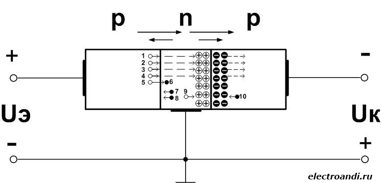
Under the action of voltage Ue, the emitter junction is shifted in the forward direction. As is known, when the electron-hole transition is forward biased, the external field is directed opposite to the transition field and therefore reduces it. The main carriers begin to pass through the transition, in the emitter these are holes 1-5, and in the base electrons 7-8. And since the number of holes in the emitter is greater than the number of electrons in the base, the emitter current is mainly due to them.
The emitter current is the sum of the hole component of the emitter current and the electronic component of the base.
![]()
Since only the hole component is useful, they try to make the electronic component as small as possible. The qualitative characteristic of the emitter junction is injection ratio.
They try to bring the injection coefficient closer to 1.
Holes 1-5 that have passed into the base accumulate on the border of the emitter junction. Thus, a high concentration of holes is created near the emitter and a low concentration near the collector junction, as a result of which the diffusion movement of holes from the emitter to the collector junction begins. But near the collector junction, the hole concentration remains zero, because as soon as the holes reach the junction, they are accelerated by its internal field and are extracted (drawn) into the collector. Electrons are repelled by this field.
While the holes cross the base layer, they recombine with the electrons located there, for example, as hole 5 and electron 6. And since the holes are constantly coming in, they create an excess positive charge, therefore, electrons must also come in, which are drawn through the base terminal and form the base current Ibr. This is an important condition for the operation of the transistor – the concentration of holes in the base should be approximately equal to the concentration of electrons. In other words the electrical neutrality of the base must be ensured.
The number of holes that have reached the collector is less than the number of holes that have left the emitter by the amount of recombined holes in the base. That is, The collector current differs from the emitter current by the base current.
![]()
From here comes transfer coefficient carriers, which they also try to bring closer to 1.
The collector current of the transistor consists of the hole component Icr and the collector reverse current.
![]()
The reverse collector current occurs as a result of the reverse bias of the collector junction, therefore it consists of minority carriers of a hole 9 and an electron 10. It is precisely because the reverse current is formed by minority carriers that it depends only on the thermal generation process, that is, on temperature. Therefore, it is often called thermal current.
The quality of the transistor depends on the magnitude of the thermal current, the smaller it is, the better the transistor is.
The collector current is coupled to the emitter current transfer ratio.
The currents in a transistor can be represented as follows

Basic ratio for transistor currents
![]()
The collector current can be expressed as
![]()
From the above, it can be concluded that By changing the current in the base-emitter circuit, we can control the collector output current. Moreover, a slight change in the base current causes a significant change in the collector current.
Depending on the principle of operation and design features, transistors are divided into two large classes: bipolar and field.
bipolar transistor- This is a semiconductor device with two interacting pn junctions and three or more conclusions.
The semiconductor crystal of a transistor consists of three regions with alternating types of electrical conductivity, between which there are two r-p-transition. The middle region is usually made very thin (fractions of a micron), so r-p transitions are closely spaced from one another.
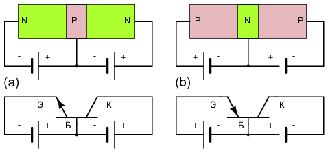
Depending on the order of alternation of semiconductor regions with various types electrical conductivity distinguish transistors r-p-r and p-r-p- types . Simplified structures and UGOs different types transistors are shown in figure 1.23, a, b.
Figure 1.23 - Structure and UGO of bipolar transistors
The bipolar transistor is the most common active semiconductor device. Silicon is currently used as the main material for the manufacture of bipolar transistors. In this case, transistors are mainly manufactured p-r-p-type, in which the main charge carriers are electrons having a mobility two to three times higher than the mobility of holes.
The control of the value of the current flowing in the output circuit (in the collector or emitter circuit) of the bipolar transistor is carried out using current in the circuit of the control electrode - base. base called average layer in the transistor structure. The outer layers are called emitter (to emit, eject) and collector (gather). The concentration of impurities (and, consequently, the main charge carriers) in the emitter is much higher than in the base and higher than in the collector. Therefore, the emitter region is the most low-resistance.
To illustrate the physical processes in the transistor, we use the simplified structure of the transistor p-r-p- type shown in Figure 1.24. To understand the principle of operation of a transistor, it is extremely important to consider that r-p Transistor junctions strongly interact with each other. This means that the current of one junction strongly affects the current of the other, and vice versa.
In active mode (when the transistor works as an amplifying element), two power supplies are connected to the transistor in such a way that emitter transition has been moved forward, a collector - in the opposite(Figure 1.24). Under the action of the electric field of the source E BE through the emitter junction flows a sufficiently large forward current I E, which is provided mainly by injection electrons from the emitter into the base The injection of holes from the base into the emitter will be insignificant due to the above difference in the concentrations of impurity atoms.
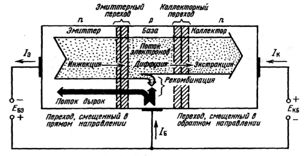
Figure 1.24 - Physical processes in a bipolar transistor
Electron flow providing current I E through the transition emitter - base is shown in Figure 1.24 with a wide arrow. Part of the electrons injected into the base region (1 ... 5%) recombine with the main charge carriers for this region - holes, forming a current in the external circuit of the base I B. Due to the large difference in the concentrations of the main charge carriers in the emitter and base, uncompensated electrons injected into the base move deep into it towards the collector.
Near the collector r-p- transition electrons are subjected to an accelerating electric field this reverse biased transition. And since they are minor carriers in the database, it happens retraction (extraction ) electrons into the collector region. In the collector, the electrons become the main charge carriers and easily reach the collector terminal, creating a current in the external circuit of the transistor.
In this way, current through the base terminal of the transistor is determined by two oppositely directed current components. If there were no recombination processes in the base, then these currents would be equal to each other, and the resulting base current would be equal to zero. But since recombination processes are present in any real transistor, the emitter current pn-transition slightly more than the collector current pn-transition.
For the collector current, we can write the following equation
![]() , (1.9)
, (1.9)
where a st- static emitter current transfer coefficient;
I KBO- reverse current of the collector junction (thermal current) (for low power transistors at normal temperature it is 0.015 ... 1 μA).
In practice, the static emitter current transfer coefficient a st, depending on the type of transistor, can take values in the range of 0.95 ... 0.998.
The emitter current in the transistor is numerically the largest and is equal to
, (1.11)
where is the static current transfer coefficient of the base in a circuit with a common emitter (in the reference literature, the designation is used h 21E, usually takes the value b st= 20 ... 1000 depending on the type and power of the transistor).
It follows from the above that the transistor is a controlled element, since the value of its collector (output) current depends on the values of the emitter and base currents.
Finishing the consideration of the principle of operation of a bipolar transistor, it should be noted that the resistance of a reverse-biased collector junction (when a reverse voltage is applied to it) is very high (hundreds of kilo-ohms). That's why in the collector circuit, you can include load resistors with very great resistance , thereby practically not changing the value of the collector current. Accordingly, significant power will be allocated in the load circuit.
The resistance of a forward-biased emitter junction, on the contrary, is very small (tens to hundreds of ohms). Therefore, at almost the same values emitter and collector currents, the power consumed in the emitter circuit turns out to be significantly less than the power released in the load circuit. This indicates that A transistor is a semiconductor device that amplifies power..
The manufacturing technology of bipolar transistors can be different: fusion, diffusion , epitaxy. This largely determines the characteristics of the device. Typical structures of bipolar transistors manufactured various methods are shown in Figure 1.25. In particular, in figure 1.25, a shown structure floatable, in figure 1.25, b - epitaxially-diffusion, in figure 1.25, in - planar, in figure 1.25, G - mesaplanar transistors.
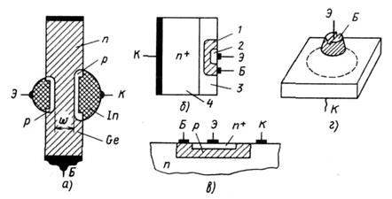
Figure 1.25 - Methods for manufacturing bipolar transistors
Operating modes and transistor switching circuits
For each r-p- the transistor junction can be fed both forward and reverse voltage. In accordance with this, four modes of operation of a bipolar transistor are distinguished: mode cut-off, mode saturation, active mode and inverse mode.
Active the mode is provided by supplying a direct voltage to the emitter junction, and a reverse voltage to the collector junction (the main operating mode of the transistor). This mode corresponds to the maximum value of the emitter current transfer coefficient and ensures minimum distortion of the amplified signal.
AT inverse mode, a forward voltage is applied to the collector junction, and a reverse voltage is applied to the emitter junction (a st®min; very rarely used).
In mode saturation both junctions are under forward bias. In this case, the output current does not depend on the input current and is determined only by the load parameters.
In mode cut-off both junctions are reverse-biased. The output current is close to zero.
Saturation and cutoff modes are used simultaneously in key schemes(when the transistor is operating in the key mode).
When using a transistor in electronic devices, two pins are needed to supply the input signal and two pins to connect the load (remove the output signal). Since the transistor has only three pins, one of them must be common to the input and output signals.
Depending on which output of the transistor is common when connecting the signal source and load, there are three transistor switching schemes: with common base(OB) (Figure 1.26, a); With common emitter(OE) (Figure 1.26, b); With common collector(OK) (Figure 1.26, in).
In these diagrams, sources constant voltage and resistors provide the operating modes of transistors for direct current, that is, the necessary values of voltages and initial currents. AC input signals are generated by sources and in. They change the emitter (base) current of the transistor, and, accordingly, the collector current. Collector current increments (Figure 1.26, a, b) and emitter current (Figure 1.26, in) will create, respectively, on resistors R K and R E voltage increments, which are the output signals and out.
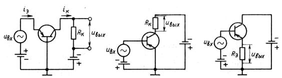
a B C
Figure 1.26 - Transistor switching circuits
When determining the transistor switching circuit, it is necessary to take into account the fact that the resistance of the DC voltage source for AC is close to zero.
Current-voltage characteristics of the transistor
The properties of a bipolar transistor are most fully described using static current-voltage characteristics. In this case, the input and output I–V characteristics of the transistor are distinguished. Since all three currents (base, collector and emitter) in a transistor are closely interconnected, when analyzing the operation of a transistor, it is necessary to use both input and output I–V characteristics.
Each switching circuit of the transistor has its own current-voltage characteristics, which are the functional dependence of the currents through the transistor on the applied voltages. Due to the non-linear nature of these dependencies, they are usually presented in graphical form.
The transistor, as a quadripole, is characterized input and weekend static I–V characteristics, showing, respectively, the dependence of the input current on the input voltage (at a constant value of the output voltage of the transistor) and the output current on the output voltage (at a constant input current of the transistor).
Figure 1.27 shows the static I–V characteristics r-p-r-transistor connected according to the scheme with OE (the most commonly used in practice).
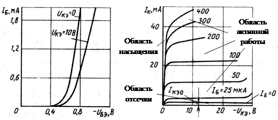
a b
Figure 1.27 - Static IV characteristics of a bipolar transistor connected according to the circuit with OE
Input CVC (Figure 1.27, a) is similar to the direct branch of the CVC of the diode. It represents the dependence of the current I B from voltage U BE U CE, that is, a dependence of the form
 . (1.12)
From figure 1.27, a It can be seen that the higher the voltage U CE, the more to the right the branch of the input CVC is shifted. This is because as the reverse bias voltage increases, U CE there is an increase in the height of the potential barrier of the collector R-P-transition. And since in a transistor the collector and emitter R-P-junctions interact strongly, this, in turn, leads to a decrease in the base current at a constant voltage U BE.
Static IV characteristics, presented in Figure 1.27, a taken at normal temperature (20°C). As the temperature rises, these characteristics will shift to the left, and as they fall, they will shift to the right. This is due to the fact that with increasing temperature, the intrinsic electrical conductivity of semiconductors increases.
For the output circuit of a transistor connected according to the OE circuit, a family of output I–V characteristics is built (Figure 1.27, b). This is due to the fact that the collector current of the transistor depends not only (and not so much, as can be seen from the figure) on the voltage applied to the collector junction, but also on the base current. Thus, the output current-voltage characteristic for a circuit with OE is the dependence of the current I K from voltage U CE at fixed current I B, that is, a dependence of the form
 . (1.13)
Each of the output I–V characteristics of a bipolar transistor is characterized at the beginning by a sharp increase in the output current I K with increasing output voltage U CE, and then, as the voltage increases further, a slight change in current.
Three regions can be distinguished on the output I–V characteristic of the transistor, corresponding to different operating modes of the transistor: saturation, region cut-off and region active work(gain) , corresponding to the active state of the transistor, when ½ U BE½ > 0 and ½ U CE½> 0.
The input and output static I–V characteristics of transistors are used in the graph-analytical calculation of cascades containing transistors.
Static input and output IV characteristics of a bipolar transistor R-P-R-type for the switching circuit with OB are shown in Figure 1.28, a and 1.28, b respectively.

a b
Figure 1.28 - Static IV characteristics of a bipolar transistor for a switching circuit with ABOUT
For a circuit with ABOUT the input static I–V characteristic, the current dependence is called I E from voltage U EB at a fixed voltage value U KB, that is, a dependence of the form
 . (1.14)
The output static I–V characteristic for a circuit with OB is called the current dependence I K from voltage U KB at fixed current I E, that is, a dependence of the form
 . (1.15)
In figure 1.28, b two regions can be distinguished, corresponding to two modes of operation of the transistor: active mode ( U KB< 0 и коллекторный переход смещен в обратном направлении); режим saturation(U KB > 0 and the collector junction is forward biased).
Mathematical model of a bipolar transistor
To date, many electrical models of bipolar transistors are known. In design automation systems (CAD) of electronic means, the most commonly used are: Ebers-Moll models, the generalized Hummel-Poon charge control model, the Linville model, as well as Giacolleto's local P- and T-shaped models of linear increments.
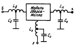
Consider, as an example, one of the variants of the Ebers-Moll model (Figure 1.29), which reflects the properties of the transistor structure in the linear mode of operation and in the cutoff mode.
 |
Figure 1.29 - Bipolar transistor equivalent circuit (Ebers-Moll model)
Figure 1.29 uses the notation: r e, r b, r to- resistance, respectively, of the emitter, base and collector regions of the transistor and contacts to them; I b , I to - voltage controlled at the input junction, current sources reflecting the transfer of current through the transistor; R eb- leakage resistance of the base-emitter junction; R kb - leakage resistance of the base-collector junction. Source current I b is related to the voltage at the junction by the relation
 , (1.15)
where I BO- saturation current of the base-emitter transition (reverse current);
y to= (0.3 ... 1.2) V - contact potential difference (depends on the type of semiconductor material);
t- empirical coefficient.
Parallel to the base-emitter junction included barrier capacity C bae and diffusion capacity C de transition. Value C bae determined reverse voltage at the crossing and n and legally dependent on him
 , (1.16)
where С 0 b - transfer capacitance at and n = 0;
g = 0.3 ... 0.5 - coefficient depending on the distribution of impurities in the base region of the transistor.
Diffusion capacity is a function of the current I b, flowing through the transition, and is determined by the expression
where BUT - coefficient depending on the properties of the transition and its temperature.
The collector-base junction is modeled similarly, the only difference is that only the barrier capacitance of the junction is taken into account
 , (1.18)
since when the transistor is operating in a linear mode and in the collector current cut-off mode, this transition is closed. Expression for current controlled collector current source, modeling the amplifying properties of the transistor, has the form
 , (1.19)
where b st- static current transfer coefficient of the base of the transistor in a circuit with a common emitter.
The parameters of the Ebers-Moll model can be obtained either by calculation based on the analysis of the physico-topological model of the transistor, or measured experimentally. The static parameters of the model are most easily determined at direct current.
 |
Global the electrical model of a discrete bipolar transistor, taking into account the inductance and capacitance of its outputs, is shown in Figure 1.30.
Figure 1.30 - Global model of a bipolar transistor
Basic parameters of a bipolar transistor
When determining the variable components of currents and voltages (that is, when analyzing electrical circuits on the alternating current) and provided that the transistor is in active mode, it is often represented as a linear quadripole (Figure 1.31, a). The names (physical essence) of the input and output currents and voltages of such a four-terminal network depend on the transistor switching circuit.
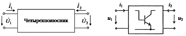
a b
Figure 1.31 - Representation of a bipolar transistor by a linear quadripole
For the switching circuit of a transistor with a common emitter, the currents and voltages of the quadripole (Figure 1.31, b) correspond to the following transistor currents and voltages:
- i 1 - variable component of the base current;
- u 1 - variable component of the voltage between the base and the emitter;
- i 2 - variable component of the collector current;
- u 2 - the variable component of the voltage between the collector and emitter.
The transistor is conveniently described using the so-called h-options. In this case, the system of equations of the quadripole in matrix form takes the form
 . (1.20)
Odds h ij(that is h-parameters) define empirically, using in turn the short circuit and idle modes at the input and output of the quadripole.
Essence h- parameters for the switching circuit of a transistor with OE is as follows:
-  - input resistance of the transistor for a variable signal with a short circuit at the output;
-  - output conductivity of the transistor at idle at the input;
-  - voltage feedback coefficient at no-load at the input;
-  - current transfer coefficient of the transistor in case of a short circuit at the output.
Using the transistor equivalent circuit, you can find the dependence h-parameters from transistor parameters.
In particular, it can be shown that for the switching circuit of a transistor with OE, the following relations take place:
In the above formulas, following options transistors:
- r b- ohmic resistance of the base body. For real transistors, it reaches values of 100 ... 200 Ohms;
- r e- resistance R-P-transition, the value of which depends on the operating mode of the transistor and changes in the active mode within fractions - tens of ohms;
B- differential factor base current transmission, determined from the expression
 ; (1.25)
Collector region resistance, determined from the expression
 , (1.26)
where r to- differential resistance of the collector junction (usually within a fraction - tens of MΩ), determined from the expression
 (1.27)
Added October 21, 2016 at 05:45 pm
Chapter 2 - Theory of Solid State Devices
The bipolar transistor was so named because its operation involves the movement of two charge carriers: electrons and holes in the same crystal. The first bipolar transistor was invented at Bell Labs by William Shockley, Walter Brattain, and John Bardeen in late 1947, and so was not published until 1948. Thus, many texts differ on the date of invention. Brattain made a germanium point transistor, which bore some resemblance to a point diode. Within a month, Shockley had a more practical junction bipolar transistor, which we describe below. In 1956, for the invention of the transistor, they were awarded Nobel Prize in physics.
The bipolar transistor shown in Figure below (a) is an NPN three-layer semiconductor sandwich with an emitter and collector at the ends and a base in between. It is as if a third layer was added to a two-layer diode. But if that were the only requirement, a pair of back-to-back diodes would suffice. And it’s much easier to make a pair of diodes located “back to back”. But the basis of making a bipolar transistor is to make the middle layer, the base, as thin as possible without shorting the outer layers, emitter and base. The importance of the thin base area cannot be overemphasized.
The semiconductor device in Figure below (a) has two junctions, between emitter and base and between base and collector, and two depletion regions.
(a) Bipolar NPN transistor.
(b) Applying a reverse bias to the base-collector junction.
It is customary to apply a reverse bias to the base-collector junction of a bipolar transistor, as shown in figure above (b). Note that this increases the width of the depletion region. The reverse bias voltage for most transistors can range from a few volts to tens of volts. There is currently no current in the collector circuit other than leakage current.
In figure below (a), another voltage source has been added to the circuit between emitter and base. Typically, we apply a forward bias to the emitter-base junction that overcomes the potential barrier of 0.6V. It's like a forward shift semiconductor diode. The voltage source must exceed 0.6V in order for the majority carriers (electrons for NPN) to start flowing from the emitter to the base, becoming minority charge carriers in the P-type semiconductor.
If the base region were thick, as in a pair of back-to-back diodes, all the current flowing into the base would flow through the base lead. In our example NPN transistor, the electrons exiting the emitter into the base will combine with the holes in the base, making room for more holes to be created on the (+) terminal of the battery connected to the base once the electrons have left.
However, the base is made thin. Several majority carriers in the emitter introduced as minority carriers into the base actually recombine. See figure below (b). Several electrons introduced by the emitter into the base of the NPN transistor fall into the holes. Also, a few electrons that enter the base will flow directly through the base to the positive terminal of the battery. Most of the emitter electron flux diffuses through the thin base into the collector. In addition, a small change in the base current results in a large change in the collector current. If the base voltage drops below about 0.6 volts for a silicon transistor, then it stops flowing. high current emitter-collector.
 Collector-Base Reverse Bipolar NPN Bipolar Transistor: (a) Adding forward bias to the base-emitter junction results in (b) low base current and high emitter and collector currents.
 In the figure below, we take a closer look at the current amplification mechanism. We have an enlarged view of the junctions of an NPN bipolar transistor with an emphasis on the thin base region. Although not shown, we assume that external voltage sources are connected: (1) forward-biased emitter-base junction, (2) reverse-biased base-collector junction. Electrons, the majority carriers, enter the emitter from the (-) terminal of the battery. The base current corresponds to the electrons leaving the base terminal to the (+) terminal of the battery. However, this is a small current compared to the emitter current.
 Electrons included in the base:
 (a) Lost due to recombination with base holes.
(b) Outgoing base output.
(c) Most diffuse from the emitter through the thin base into the base-collector depletion region,
and (d) are quickly captured by the strong depletion region electric field into the collector.
Majority carriers inside an N-type emitter are electrons that become minority carriers when they enter a P-type base. These electrons hitting the P-type thin base have four possibilities. A few electrons (in figure (a) above) enter holes in the base, which allows current to flow to the base terminal from the (+) terminal of the battery. This is not shown, but holes in the base can diffuse into the emitter and combine with electrons, allowing current to flow through the base lead. Several (b) flow through the base to the (+) terminal of the battery, as if the base were just a resistor. Both groups of electrons (a) and (b) contribute very little to the base current. For low power transistors, the base current is typically 1% of the emitter or collector current. Most of the emitter electrons diffuse through the thin base (c) into the base-collector depletion region. Note the polarity of the depletion region surrounding the electron in (d). A strong electric field quickly sweeps the electron into the collector. The field strength is proportional to the collector battery voltage. Thus, 99% of the emitter current goes to the collector. It is controlled by the base current, which is 1% of the emitter current. This is a potential current amplification of 99 times, the ratio I K / I B, also known as beta β.
This is amazing, 99% of the emitter carriers propagating through the base is only possible if the base is very thin. What would happen to the main emitter carriers if the base were 100 times thicker? One would expect an increase in recombination, the number of electrons falling into holes would be much larger. Maybe 99%, not 1%, would have gotten into the holes, never reaching the collector. The second point is that the base current can drive 99% of the emitter current only if 99% of the emitter current diffuses into the collector. If all the current flowed from the base, no control would be possible.
Another feature required to transfer 99% of the electrons from the emitter to the collector is that real bipolar transistors use a small heavily doped emitter. The high concentration of emitter electrons causes more electrons to diffuse into the base. The lower dopant concentration in the base means that fewer holes diffuse into the emitter, which could increase the base current. The propagation of charge carriers from the emitter to the base enjoys a great advantage.
The thin base and heavily doped emitter help keep the emitter efficiency high, such as 99%. This corresponds to 100% of the emitter current being shared between base (1%) and collector (99%). The emitter efficiency is known as α = I K / I E.
Bipolar transistors can have both NPN and PNP structures. We will compare these two structures in the figure below. The difference lies in the polarity of the base-emitter PN junctions, which is indicated by the direction of the emitter arrow on the symbol. It points in the same direction as the arrow on the anode of the diode, opposite to the direction of the electrons.
See the symbol on the image in P-N transition. The beginning of the arrow and its end correspond to P-type and N-type semiconductors, respectively. For NPN and PNP emitters, the arrow points from the base to the base, respectively. There is no arrow on the manifold on the symbol. However, the base-collector junction has the same polarity as the diode as the base-emitter junction. Note that we are talking about the polarity of the diode, not the power supply.
 Compare an NPN transistor (a) with a PNP transistor (b). Pay attention to the emitter arrow and the polarity of the power supply.
 The voltage sources for PNP transistors are reversed compared to NPN transistors, as shown in the figure above. The base-emitter junction must be forward biased in both cases. The base of the PNP transistor is biased negatively (b), compared to positive (a) for the NPN transistor. In both cases, the base-collector junction is biased in the opposite direction. The collector power supply of a PNP transistor has a negative polarity, compared to the positive polarity for an NPN transistor.
 Bipolar Junction Transistor (BJT): (a) individual device cross section, (b) symbol, (c) integrated circuit cross section.
 Note that the bipolar transistor (BJT) in Figure (a) above has a heavily doped emitter, denoted N+. The base has a normal level of P-doping. The base is much thinner than shown in the cross section not to scale. The collector is lightly doped, which is indicated by N - . The collector must be doped so lightly that the collector-base junction has high voltage breakdown. This results in a high allowable collector power supply voltage. The breakdown voltage for low-power silicon transistors is 60-80 volts. For high-voltage transistors, it can reach hundreds of volts. The collector must also be heavily doped to reduce resistive losses if the transistor is to handle high currents. These conflicting requirements are met by a stronger alloying of the collector in the area of the metal contact. The collector near the base is lightly doped compared to the emitter. Heavy doping in the emitter results in a low emitter-base junction breakdown voltage, which is about 7 volts for low power transistors. The heavily doped emitter makes the reverse-biased emitter-base junction similar in performance to a zener diode.
The base of a bipolar junction transistor, a semiconductor plate, is a collector mounted (in the case of high-power transistors) on a metal case. That is, the metal case is electrically connected to the collector. The base of low power transistors can be encapsulated in epoxy. In high-power transistors, aluminum connecting wires are connected to the base and emitter and connected to the body leads. Bases of low-power transistors can be installed directly on the output conductors. Several transistors can be made on one chip, which will be called an integrated circuit. The collector can even be installed not on the case, but on the output. An integrated circuit may contain internal conductors connecting transistors and other integrated components. The built-in bipolar transistor shown in figure (c) above is much thinner than shown in the "not to scale" figure. The P+ region isolates multiple transistors in a single chip. An aluminum plating layer (not shown) interconnects several transistors and other components. The emitter region is heavily doped with N+ compared to the base and collector in order to increase emitter efficiency.
Discrete PNP transistors are almost as high quality as NPN transistors. However, integrated PNP transistors are not as good as NPNs in a similar integrated circuit chip. Thus, integrated circuits use NPN transistors to the maximum.
Summing up
- Bipolar transistors conduct current using both electrons and holes in the same device.
- The operation of a bipolar transistor as a current amplifier requires that the collector-base junction be reverse-biased and the emitter-base junction be forward-biased.
- A transistor differs from a pair of back-to-back diodes in that the base (center layer) is very thin. This allows the majority charge carriers from the emitter to diffuse, as minority carriers, through the base into the depletion region of the base-collector junction, where they are picked up by a strong electric field.
- The emitter efficiency is improved by heavier doping compared to the collector. Emitter efficiency: α = I C / I E , is 0.99 for low power transistors.
- Current gain: β=I C /I B , for low power transistors is in the range from 100 to 300.
If we consider mechanical counterparts, then the operation of transistors resembles the principle of operation of a hydraulic power steering in a car. But, the similarity is valid only at a first approximation, since there are no valves in transistors. In this article, we will separately consider the operation of a bipolar transistor.
Bipolar transistor device
The basis of the bipolar transistor device is a semiconductor material. The first semiconductor crystals for transistors were made from germanium, today silicon and gallium arsenide are more commonly used. First, a pure semiconductor material is produced with a well-ordered crystal lattice. Then the crystal is given the necessary shape and a special impurity is introduced into its composition (material is alloyed), which gives it certain properties of electrical conductivity. If the conductivity is due to the movement of excess electrons, it is defined as donor (electronic) n-type. If the conductivity of a semiconductor is due to the successive replacement of vacant places, the so-called holes, by electrons, then such conductivity is called acceptor (hole) and is denoted by p-type conductivity.
Picture 1.
The transistor crystal consists of three parts (layers) with serial alternation of the type of conductivity (n-p-n or p-n-p). Transitions from one layer to another form potential barriers. The transition from base to emitter is called emitter(EP), to the collector - collector(KP). Figure 1 shows the transistor structure as symmetrical, idealized. In practice, during production, the sizes of the regions are significantly asymmetric, approximately as shown in Figure 2. The collector junction area significantly exceeds the emitter junction. The base layer is very thin, on the order of a few microns.
Figure 2.
The principle of operation of a bipolar transistor
Any p-n junction of a transistor works similarly. When a potential difference is applied to its poles, its "shift" occurs. If the applied potential difference is conditionally positive, and the p-n junction opens, the junction is said to be forward-biased. When a conditionally negative potential difference is applied, the transition is reverse-biased, at which it is locked. A feature of the transistor operation is that with a positive bias of at least one transition, the common area, called the base, is saturated with electrons, or electronic vacancies (depending on the type of conductivity of the base material), which causes a significant decrease in the potential barrier of the second transition and, as a result, its conductance under reverse bias.
Operating modes
All transistor switching circuits can be divided into two types: normal and inverse.
Figure 3
Normal transistor switching circuit involves changing the electrical conductivity of the collector junction by controlling the offset of the emitter junction.
Inverse circuit, in contrast to normal, allows you to control the conductivity of the emitter junction by controlling the bias of the collector. The inverse circuit is a symmetrical analog of the normal one, but due to the structural asymmetry of the bipolar transistor, it is ineffective for use, has more stringent restrictions on the maximum allowable parameters and is practically not used.
With any switching scheme, the transistor can operate in three modes: Cutoff mode, active mode and saturation mode.
To describe the job direction electric current in this article, it is conditionally taken as the direction of electrons, i.e. from the negative pole of the power supply to the positive. Let's use the diagram in Figure 4 for this.
Figure 4
Cutoff mode
For the p-n junction, there is a value for the minimum forward bias voltage at which electrons are able to overcome the potential barrier of this junction. That is, at a forward bias voltage up to this threshold, no current can flow through the junction. For silicon transistors, the value of such a threshold is approximately 0.6 V. Thus, in a normal switching circuit, when the forward bias of the emitter junction does not exceed 0.6 V (for silicon transistors), no current flows through the base, it is not saturated with electrons, and as a consequence, there is no emission of base electrons into the collector region; there is no collector current (zero).
Thus, for the cutoff regime, the following identities are a necessary condition:
U BE<0,6 В
I B \u003d 0
Active Mode
In the active mode, the emitter junction is biased in the forward direction until the moment of unlocking (the start of current flow) with a voltage of more than 0.6 V (for silicon transistors), and the collector junction is biased in the opposite direction. If the base has p-type conductivity, there is a transfer (injection) of electrons from the emitter to the base, which are instantly distributed in a thin layer of the base and almost all of them reach the collector boundary. The saturation of the base with electrons leads to a significant decrease in the size of the collector junction, through which the electrons, under the action of a negative potential from the emitter and base, are displaced into the collector region, flowing down through the collector terminal, thereby causing the collector current. The very thin layer of the base limits its maximum current passing through a very small cross section in the direction of the base lead. But this small thickness of the base causes its rapid saturation with electrons. The junction area has a significant size, which creates conditions for the flow of a significant emitter-collector current, which is tens and hundreds of times higher than the base current. Thus, by passing insignificant currents through the base, we can create conditions for the passage of much larger currents through the collector. The greater the base current, the greater its saturation, and the greater the collector current. This mode allows you to smoothly control (regulate) the conductivity of the collector junction by a corresponding change (regulation) of the base current. This property of the active mode of the transistor is used in the circuits of various amplifiers.
In active mode, the emitter current of the transistor is the sum of the base and collector currents:
I E \u003d I K + I B
Collector current can be expressed as:
I K = α I E
where α is the emitter current transfer coefficient
From the above equations, you can get the following:
![]()
where β is the base current amplification factor.
Saturation mode
The limit of the increase in the base current until the moment when the collector current remains unchanged determines the point of maximum saturation of the base with electrons. A further increase in the base current will not change the degree of its saturation, and in no way will affect the collector current, it can lead to overheating of the material in the base contact area and failure of the transistor. In the reference data for transistors, the saturation current and the maximum allowable base current, or the emitter-base saturation voltage and the maximum allowable emitter-base voltage, can be indicated. These limits determine the saturation mode of the transistor under normal operating conditions.
The cutoff mode and saturation mode are effective when transistors operate as electronic switches for switching signal and power circuits.
The difference in the principle of operation of transistors with different structures
The case of work was considered above transistor n-p-n structures. P-n-p transistors work in a similar way, but there are fundamental differences that you should be aware of. A semiconductor material with p-type acceptor conductivity has a relatively low electron transmission capacity, since it is based on the principle of electron transition from one vacancy (hole) to another. When all vacancies are replaced by electrons, their movement is possible only as vacancies appear from the direction of motion. With a significant length of the section of such a material, it will have significant electrical resistance, which leads to big problems when it is used as the most massive collector and emitter of bipolar transistors. pnp type than when used in a very thin base layer of NPN transistors. The n-type donor semiconductor material has the electrical properties of conductive metals, which makes it more advantageous to use as an emitter and collector, as in n-p-n type transistors.
This distinctive feature of the various structures of bipolar transistors leads to great difficulties in the production of pairs of components with different structures and electrical characteristics similar to each other. If you pay attention to the reference data of the characteristics of pairs of transistors, you will notice that when the same characteristics of two transistors of various types, for example, KT315A and KT361A, are achieved, despite their identical collector power (150 mW) and approximately the same current gain (20-90) , they differ in the maximum allowable collector currents, emitter-base voltages, etc.
P.S. This description of the principle of operation of the transistor was interpreted from the standpoint of Russian Theory, so there is no description of the action of electric fields on fictitious positive and negative charges. Russian Physics makes it possible to use simpler, more understandable mechanical models that are closest to reality than abstractions in the form of electric and magnetic fields, positive and electric charges, which the traditional school treacherously slips on us. For this reason, I do not recommend using the stated theory without preliminary analysis and reflection when preparing for the delivery of control, term papers and other types of work, your teachers may simply not accept dissent, even competitive and quite consistent from the point of view of common sense and logic. In addition, for my part, this is the first attempt to describe the operation of a semiconductor device from the standpoint of Russian Physics, which can be refined and supplemented in the future.
We advise you to read
 Psychological characteristics of children in adolescence
 Transferring a child to another school - the procedure and necessary documents Whether to transfer a child to another school
, diagnosis, treatment Treatment of urogenital chlamydia") Chlamydia urogenital - description, causes, symptoms (signs), diagnosis, treatment Treatment of urogenital chlamydia
Chlamydia urogenital - description, causes, symptoms (signs), diagnosis, treatment Treatment of urogenital chlamydia The benefits and significance of hydroamino acid threonine for the human body L threonine what