Voltage step down direct current. How a step down converter works. Where does it apply. Description of the operating principle. Step-by-step instruction for design (10+)
Step-down pulse voltage converter. Design. Calculation
To reduce the DC voltage with minimal losses and obtain a stabilized output, the following approach is used. The constant voltage is converted into pulses of variable duty cycle. These pulses are then passed through an inductor. Energy is stored in a storage capacitor. Feedback monitors the stability of the output voltage and for this regulates the duty cycle of the pulses.
If there is no need to reduce losses, then a series continuous stabilizer is used.
The principle of operation of a step-down voltage converter is based on the property of an inductor (choke) to accumulate energy. The accumulation of energy is manifested in the fact that the current through the inductor, as it were, has inertia. That is, it cannot change instantly. If a voltage is applied to the coil, then the current will gradually increase; if a reverse voltage is applied, the current will gradually decrease.
To your attention a selection of materials: In the diagram, we see that the control unit D1 depending on the voltage across the capacitor C2 closes and opens the power switch. Moreover, the higher the voltage C2, the shorter the time for which the key closes, that is, the lower the duty cycle (the greater the duty cycle). If the voltage across the capacitor C2 exceeds a certain value, then the key stops closing altogether until the voltage decreases. How this operation of the control circuit is ensured is described in the article on pulse-width modulation. When the power switch is closed, the current follows the path S1. In this case, a voltage is applied to the inductor, equal to the difference between the input and output voltage. The current through the coil increases in proportion to the voltage applied to the coil and the time for which the switch closes. The coil stores energy. The flowing current charges the capacitor C2. When the power switch is open, the current follows the path S2 through a diode. An output voltage with the opposite sign is applied to the inductor. The current through the coil decreases in proportion to the voltage applied to the coil and the time during which the switch is open. The current flowing still charges the capacitor C2. When the capacitor C2 charged, the key stops closing, the capacitor stops charging. The key will start to close again when the capacitor C2 slightly discharged under load. Capacitor C1 is needed in order to reduce the current ripple in the input circuit, to select from it not a pulsed, but an average current. Advantages, disadvantages, applicabilityEnergy losses directly depend on the ratio of input and output voltages. So a buck converter can theoretically generate a large output current at a low voltage from a small input current but a large voltage, but we have to interrupt high current at high voltage, which guarantees high switching losses. So buck converters are used if the input voltage is 1.5 - 4 times the output voltage, but they try not to use them with a larger difference. We will analyze the process of designing and calculating a step-down converter and test it with examples. At the end of the article there will be a form in which you can fill in the necessary source parameters, conduct an online calculation and get the denominations of all elements. Let's take the following diagrams as an example:
One of the problems of buck converters is the difficulty of controlling the power switch, since its emitter (source) is usually not connected to a common wire. Next, we will consider several options for solving this problem. For now, let's focus on a somewhat non-standard inclusion of a microcircuit - a PWM controller. We use the 1156EU3 chip. In this microcircuit, the output stage is made according to the classical push-pull circuit. The midpoint of this cascade is connected to leg 14, the emitter of the lower arm is connected to a common wire (leg 10), the collector of the upper arm is connected to leg 13. We will connect leg 14 to the common wire through a resistor, and connect leg 13 to the base of the key transistor. When the upper arm of the output stage is open (this corresponds to the supply of a triggering voltage to the output), the current flows through the emitter junction of the transistor VT2, leg 13, the upper arm of the output stage, leg 14, resistor R6. This current unlocks the transistor VT2. In such an inclusion, controllers with an open emitter at the output can also be used. These controllers do not have a lower arm. But we don't need it. In our scheme, a powerful key is used as a power key. bipolar transistor. Read more about the operation of a bipolar transistor as a power switch. A compound transistor can be used as a power switch to reduce the load on the controller. However, the saturation voltage of the collector - emitter of a composite transistor is many times greater than that of a single one. The composite transistor article describes how to calculate this voltage. If you use a composite transistor, then in the calculation form at the end of the article, indicate exactly this voltage as the saturation voltage of the collector - emitter VT2. The higher the saturation voltage, the higher the losses, so with a composite transistor, the losses will be many times greater. But there is a solution. It will be described later in the section on low power controllers. There is an output voltage. What elements does it depend on? I would also be very grateful if you could tell me how to correctly calculate the parameters of a 100v to 28v 1000 watt step-down converter. Thank you very much in advance. Microcontrollers. Compilation of the program. Schematic Design Tools |
Pulse step-up voltage converter 12 24 220 and others…
The problem of obtaining in a heavy vehicle the voltage necessary to power radio stations, car electronics and communications equipment (12-14 Volts) can be solved in several ways.
The easiest one to take required voltage from one battery. But the consequences of such "experiments" are sad: after a while, the battery will have to be thrown away. Another, "civilized" way is to install a device in the car that will allow you to get the necessary voltage without compromising the standard electrical system of the car. Currently, two types of such devices are produced that are fundamentally different from each other.
First group are linear voltage stabilizers (adapters). The essence of this type of stabilization is that the "extra" voltage "remains" on the control element. In this case, the current that flows from the battery (Iacc. Fig. 1) is equal to the current flowing into the payload (In. Fig. 1), and since the input voltage is twice the output voltage, then the power consumed from the battery is 2 times higher than the power consumed by the useful load, i.e. The efficiency of such a stabilizer (adapter) is 50% (and actually even less). Let's try to substitute live numbers for clarity. Let's take the payload current In.=20Amperes.
Raqq. = Iacc. x Uacc. = 20 A x 28 V = 560 watts
pH. = In. x Un. = 20 A x 14 V = 280 watts
The difference between these powers (280 watts) is released in the form of heat, heating the radiator of the stabilizer. To dissipate such power for a long time, a huge radiator is needed. In reality, these stabilizers (adapters) are made on radiators of much smaller sizes, which means that if the manufacturer claims that the maximum current of the stabilizer is 20 Amperes, then the stabilizer will be able to operate for a long time at a current of 6-7 Amperes, no more. These converters are optimal for powering radio stations and audio equipment. The maximum current these devices consume is just for a short time.
The second group is impulse devices. The fundamental difference between pulse circuitry is that it allows you to get power supplies with high efficiency, up to 90%. In such converters, the "extra" voltage is not dissipated in the form of heat, but is converted into an "additional" current at the output. In turn, impulse devices can be divided into two subgroups:
- switching voltage stabilizers / efficiency up to 90%
- pulse converters voltage (power supplies) / efficiency up to 80%
A distinctive feature of pulse converters is the galvanic isolation of input and output voltages (i.e. they include a transformer), which eliminates even the theoretical possibility of input voltage entering the output in case of any malfunction of the converter itself.
Modern element base and circuitry made it possible to create pulse converters and voltage stabilizers that provide:
- Long-term operation at maximum load current.
- Automatic regulation output power (you can not be afraid of overloads up to short circuit). The power limiting system will automatically detect the overload and limit the output power to a safe level.
- Due to the high efficiency, a normal thermal regime is ensured and, as a result, high reliability and small dimensions.
- The power consumed from the battery is only 10-15% more than the load consumes.
- The presence of galvanic isolation of the input and output voltages in the converter (i.e., it contains a transformer) excludes even the theoretical possibility of the input voltage getting to the output. A powerful high-performance voltage limiter is installed in the stabilizer.
- Perhaps the only drawback of pulse devices is possible radio interference, their level depends on the manufacturer (cost) of the converter. Inexpensive converters are not recommended for powering radio stations and radio receivers.
Pulse voltage converter
To transform the voltage from one level to another, pulsed DC voltage converters are used, in which inductive storage devices are used. In such converters, the output power is regulated due to changes in the time period of exposure to the load in one of two ways:
Frequency-pulse;
Pulse width.
The principle of operation of a pulsed boost voltage converter is to create such a transistor mode, during which the entire power supply circuit to the load will be periodically interrupted. Thus, the pulse converter 24 12 allows you to streamline the fluctuations in the duration of the output pulses with their unchanged period of change. A single-cycle pulse voltage converter can operate in the power range from 0 to 100 W. If a device of greater power is required, then a multi-cycle pulse voltage converter is used.
DC/DC converters are widely used to power various electronic equipment. They are used in computer technology devices, communication devices, various control and automation circuits, etc.
Transformer power supplies
In traditional transformer power supplies, the mains voltage is converted using a transformer, most often lowered, to the desired value. undervoltage straightens up diode bridge and smoothed by a capacitor filter. If necessary, a semiconductor stabilizer is placed after the rectifier.
Transformer power supplies are usually equipped with linear stabilizers. Such stabilizers have at least two advantages: this is a low cost and a small number of parts in the harness. But these advantages are eaten up by low efficiency, since a significant part of the input voltage is used to heat the control transistor, which is completely unacceptable for powering portable electronic devices.
DC/DC converters
If the equipment is powered by galvanic cells or batteries, then voltage conversion to the desired level is possible only with the help of DC / DC converters.
The idea is quite simple: constant pressure is converted into a variable, as a rule, with a frequency of several tens and even hundreds of kilohertz, increases (decreases), and then is rectified and fed into the load. Such converters are often called pulse converters.
An example is a boost converter from 1.5V to 5V, just the output voltage of a computer USB. A similar low power converter is sold on Aliexpress - http://ali.pub/m5isn.
Rice. 1. Converter 1.5V / 5V
Pulse converters are good because they have a high efficiency, within 60..90%. Another advantage of pulse converters is a wide range of input voltages: the input voltage can be lower than the output voltage or much higher. In general, DC / DC converters can be divided into several groups.
Converter classification
Lowering, in English terminology step-down or buck
The output voltage of these converters, as a rule, is lower than the input voltage: without any special losses for heating the regulating transistor, you can get a voltage of only a few volts at an input voltage of 12 ... 50V. The output current of such converters depends on the needs of the load, which in turn determines the circuit design of the converter.
Another English name for the chopper buck converter. One of the translations of this word is a breaker. In the technical literature, a buck converter is sometimes referred to as a "chopper". For now, just remember this term.
Increasing, in English terminology step-up or boost
The output voltage of these converters is higher than the input voltage. For example, with an input voltage of 5V, a voltage of up to 30V can be obtained at the output, and its smooth regulation and stabilization is possible. Quite often boost converters are called boosters.
Universal converters - SEPIC
The output voltage of these converters is held at a given level when the input voltage is either higher or lower than the input voltage. It is recommended in cases where the input voltage can vary significantly. For example, in a car, the battery voltage can vary between 9 ... 14V, and a stable voltage of 12V is required.
Inverting converters - inverting converter
The main function of these converters is to obtain an output voltage of reverse polarity relative to the power source. Very convenient in cases where bipolar power is required, for example.
All of the mentioned converters can be stabilized or unstabilized, the output voltage can be galvanically connected to the input voltage or have galvanic voltage isolation. It all depends on the specific device in which the converter will be used.
To move on to a further story about DC / DC converters, you should at least in general terms deal with the theory.
Chopper buck converter - buck type converter
Its functional diagram is shown in the figure below. The arrows on the wires show the direction of the currents.
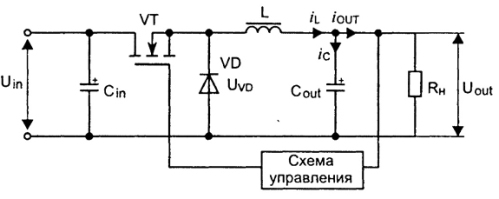
Fig.2. Functional diagram of the chopper stabilizer
The input voltage Uin is applied to the input filter - capacitor Cin. The transistor VT is used as a key element, it performs high-frequency current switching. This may be a MOSFET, IGBT, or conventional bipolar transistor. In addition to these details, the circuit contains a discharge diode VD and an output filter - LCout, from which the voltage is supplied to the load Rн.
It is easy to see that the load is connected in series with the elements VT and L. Therefore, the circuit is sequential. How does the voltage drop happen?
Pulse Width Modulation - PWM
The control circuit generates rectangular pulses with a constant frequency or a constant period, which is essentially the same thing. These pulses are shown in Figure 3.
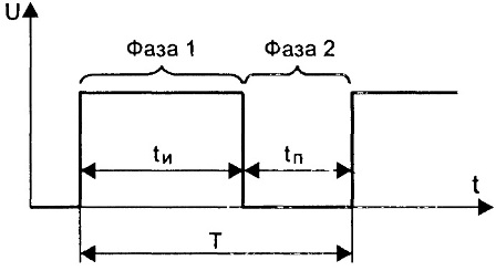
Fig.3. Control impulses
Here t is the pulse time, the transistor is open, tp is the pause time, the transistor is closed. The ratio ti/T is called the duty cycle duty cycle, denoted by the letter D and is expressed in %% or simply in numbers. For example, with D equal to 50%, it turns out that D=0.5.
Thus, D can vary from 0 to 1. With a value of D=1, the key transistor is in a state of full conduction, and with D=0 in a cutoff state, simply speaking, it is closed. It is easy to guess that at D=50% the output voltage will be equal to half of the input voltage.
It is quite obvious that the regulation of the output voltage occurs by changing the width of the control pulse t and, in fact, by changing the coefficient D. This regulation principle is called (PWM). Practically in all impulse blocks It is with the help of PWM that the output voltage is stabilized.
In the circuits shown in Figures 2 and 6, the PWM is "hidden" in boxes labeled "Control Circuit", which performs some additional functions. For example, it can be a soft start of the output voltage, remote activation or protection of the converter against a short circuit.
In general, converters received so wide application that manufacturers of electronic components have launched the production of PWM controllers for all occasions. The range is so large that it would take a whole book just to list them. Therefore, it does not occur to anyone to assemble converters on discrete elements, or as they often say in “loose” terms.
Moreover, ready-made small power converters can be bought on Aliexpress or Ebay for a small price. At the same time, for installation in an amateur design, it is enough to solder the wires to the input and output to the board, and set the required output voltage.
But back to our Figure 3. In this case, the coefficient D determines how long it will be open (phase 1) or closed (phase 2). For these two phases, the circuit can be represented by two figures. The figures DO NOT SHOW those elements that are not used in this phase.
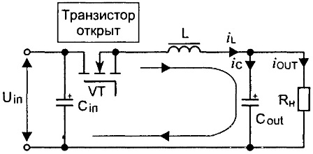
Fig.4. Phase 1
When the transistor is open, the current from the power source (galvanic cell, battery, rectifier) passes through the inductive choke L, the load Rn, and the charging capacitor Cout. In this case, current flows through the load, the capacitor Cout and the inductor L accumulate energy. The current iL GRADUALLY INCREASES due to the influence of the inductance of the inductor. This phase is called pumping.
After the voltage on the load reaches a predetermined value (determined by the setting of the control device), the transistor VT closes and the device switches to the second phase - the discharge phase. The closed transistor is not shown at all in the figure, as if it does not exist. But this only means that the transistor is closed.
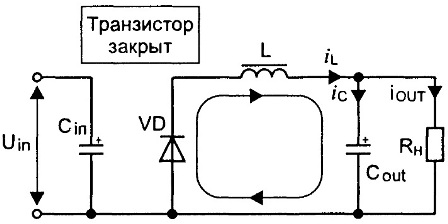
Fig.5. Phase 2
When the transistor VT is closed, there is no replenishment of energy in the inductor, since the power supply is disconnected. The inductance L tends to prevent a change in the magnitude and direction of the current (self-induction) flowing through the inductor winding.
Therefore, the current cannot stop instantly and closes through the “diode-load” circuit. Because of this, the VD diode was called a discharge diode. As a rule, this is a high-speed Schottky diode. After the control period, phase 2, the circuit switches to phase 1, the process repeats again. The maximum voltage at the output of the considered circuit can be equal to the input, and no more. Boost converters are used to obtain an output voltage greater than the input voltage.
For now, it is only necessary to recall the actual value of the inductance, which determines the two operating modes of the chopper. With insufficient inductance, the converter will operate in the mode of discontinuous currents, which is completely unacceptable for power supplies.
If the inductance is large enough, then the operation takes place in the mode of continuous currents, which allows using output filters to obtain a constant voltage with acceptable level pulsations. Boost converters also work in the continuous current mode, which will be discussed below.
For some increase in efficiency, the discharge diode VD is replaced by a MOSFET transistor, which is opened at the right time by the control circuit. Such converters are called synchronous. Their use is justified if the power of the converter is large enough.
Step-up or boost converters
Step-up converters are mainly used for low-voltage power supply, for example, from two or three batteries, and some design components require a voltage of 12 ... 15V with low current consumption. Quite often, a boost converter is briefly and clearly called the word "booster".
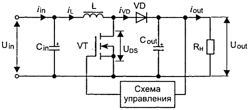
Fig.6. Functional diagram of a boost converter
The input voltage Uin is fed to the input filter Cin and fed to the series-connected L and the switching transistor VT. A VD diode is connected to the connection point of the coil and the drain of the transistor. Load Rl and shunt capacitor Cout are connected to the other terminal of the diode.
Transistor VT is controlled by a control circuit that generates a stable frequency control signal with an adjustable duty cycle D, just as described a little higher when describing the chopper circuit (Fig. 3). Diode VD at the right time blocks the load from the key transistor.
When the key transistor is open, the output of the coil L, right according to the scheme, is connected to the negative pole of the power source Uin. Increasing current (affects the influence of inductance) from the power source flows through the coil and open transistor, energy accumulates in the coil.
At this time, the diode VD blocks the load and the output capacitor from the switching circuit, thereby preventing the discharge of the output capacitor through the open transistor. The load at this moment is powered by the energy stored in the capacitor Cout. Naturally, the voltage across the output capacitor drops.
As soon as the output voltage becomes slightly lower than the specified one (determined by the settings of the control circuit), the key transistor VT closes, and the energy stored in the inductor recharges the capacitor Cout through the diode VD, which feeds the load. In this case, the self-induction EMF of the coil L is added to the input voltage and transferred to the load, therefore, the output voltage is greater than the input voltage.
When the output voltage reaches the set stabilization level, the control circuit opens the transistor VT, and the process is repeated from the energy storage phase.
Universal converters - SEPIC (single-ended primary-inductor converter or a converter with an asymmetrically loaded primary inductor).
Such converters are mainly used when the load has little power, and the input voltage changes relative to the output voltage up or down.
Fig.7. Functional diagram of the SEPIC converter
Very similar to the boost converter circuit shown in Figure 6, but with additional elements: capacitor C1 and coil L2. It is these elements that ensure the operation of the converter in the voltage reduction mode.
SEPIC converters are used in cases where the input voltage varies over a wide range. An example is 4V-35V to 1.23V-32V Boost Buck Voltage Step Up/Down Converter Regulator. It is under this name that a converter is sold in Chinese stores, the circuit of which is shown in Figure 8 (click on the picture to enlarge).

Fig.8. circuit diagram SEPIC converter
Figure 9 shows the appearance of the board with the designation of the main elements.

Fig.9. Appearance SEPIC converter
The figure shows the main parts according to figure 7. Note the presence of two coils L1 L2. By this sign, you can determine that this is a SEPIC converter.
The input voltage of the board can be within 4 ... 35V. In this case, the output voltage can be adjusted within 1.23 ... 32V. The operating frequency of the converter is 500 kHz. With small dimensions of 50 x 25 x 12 mm, the board provides power up to 25 watts. Maximum output current up to 3A.
But here a remark should be made. If the output voltage is set at 10V, then the output current cannot be higher than 2.5A (25W). With an output voltage of 5V and a maximum current of 3A, the power will be only 15W. The main thing here is not to overdo it: either do not exceed the maximum allowable power, or do not go beyond the allowable current.
To convert the voltage of one level to a voltage of another level, it is often used pulse voltage converters using inductive energy storage. Such converters are characterized by high efficiency, sometimes reaching 95%, and have the ability to obtain increased, reduced or inverted output voltage.
In accordance with this, three types of converter circuits are known: step-down (Fig. 4.1), boost (Fig. 4.2) and inverting (Fig. 4.3).
Five elements are common to all these types of converters: a power source, a key switching element, an inductive energy storage device (an inductor, a choke), a blocking diode, and a filter capacitor connected in parallel with the load resistance.
The inclusion of these five elements in various combinations allows you to implement any of the three types of pulse converters.
The output voltage level of the converter is controlled by changing the width of the pulses that control the operation of the key switching element and, accordingly, the energy stored in the inductive storage device.
The output voltage is stabilized by using feedback: when the output voltage changes, the pulse width changes automatically.
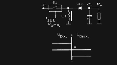
The buck converter (Fig. 4.1) contains a series-connected circuit of a switching element S1, an inductive energy storage L1, a load resistance Rн and a filter capacitor connected in parallel C1. The blocking diode VD1 is connected between the connection point of the key S1 with the energy storage L1 and a common wire.
Rice. 4.1. The principle of operation of the step-down voltage converter

Rice. 4.2. The principle of operation of the step-up voltage converter
At public key the diode is closed, the energy from the power supply is stored in the inductive energy storage. After the key S1 is closed (opened), the energy stored by the inductive storage L1 is transferred through the diode VD1 to the load resistance R n. Capacitor C1 smooths out the voltage ripple.
The step-up pulse voltage converter (Fig. 4.2) is made on the same basic elements, but has a different combination of them: a series circuit of an inductive energy storage device L1, a diode VD1 and a load resistance with a filter capacitor connected in parallel C1 is connected to the power source. The switching element S1 is connected between the connection point of the energy storage device L1 with the diode VD1 and the common bus.
When the switch is open, the current from the power source flows through the inductor, in which energy is stored. Diode VD1 is closed, the load circuit is disconnected from the power source, key and energy storage. The voltage on the load resistance is maintained due to the energy stored on the filter capacitor. When the key is opened, the self-induction EMF is added to the supply voltage, the stored energy is transferred to the load through the open diode VD1. The output voltage obtained in this way exceeds the supply voltage.
Rice. 4.3. Pulse voltage conversion with inversion
The pulse-type inverting converter contains the same combination of basic elements, but again in a different connection (Fig. 4.3): a series circuit of a switching element S1, a diode VD1 and a load resistance R n with a filter capacitor C1 is connected to the power source. The inductive energy storage L1 is connected between the connection point of the switching element S1 with the diode VD1 and the common bus.
The converter works like this: when the key is closed, energy is stored in an inductive storage device. Diode VD1 is closed and does not pass current from the power source to the load. When the switch is turned off, the self-induction EMF of the energy storage device is applied to the rectifier containing the diode VD1, the load resistance R n and the filter capacitor C1. Since the rectifier diode passes only negative voltage pulses into the load, a voltage is formed at the output of the device negative sign(inverse, opposite in sign to the supply voltage).
To stabilize the output voltage switching regulators of any type conventional "linear" regulators can be used, but they have low efficiency. In this regard, it is much more logical to use pulse voltage stabilizers to stabilize the output voltage of pulse converters, especially since such stabilization is not difficult at all.
Switching voltage stabilizers, in turn, are divided into Pulse Width Modulated Stabilizers and on stabilizers with frequency-pulse modulation. In the first of them, the duration of the control pulses changes at a constant frequency of their repetition. Secondly, on the contrary, the frequency of the control pulses changes with their duration unchanged. There are impulse stabilizers with mixed regulation.
Below, amateur radio examples of the evolutionary development of pulse converters and voltage stabilizers will be considered.
The master oscillator (Fig. 4.4) of pulse converters with unstabilized output voltage (Fig. 4.5, 4.6) on the KR1006VI1 (NE 555) chip operates at a frequency of 65 kHz. The output rectangular pulses of the generator are fed through RC circuits to transistor key elements connected in parallel.
The inductor L1 is made on a ferrite ring with an outer diameter of 10 mm and a magnetic permeability of 2000. Its inductance is 0.6 mH. The efficiency of the converter reaches 82%. The output ripple amplitude does not exceed 42 mV and depends on the capacitance value
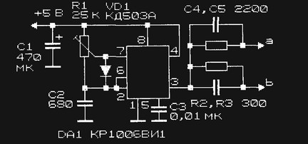
Rice. 4.4. Driving oscillator circuit for pulse voltage converters
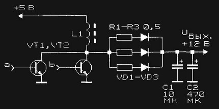
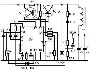
Rice. 4.5. Scheme of the power part of the step-up pulse voltage converter +5/12 V

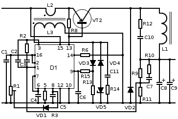
Rice. 4.6. Scheme of an inverting pulse voltage converter +5 / -12 V
capacitors at the output of the device. The maximum load current of devices (Fig. 4.5, 4.6) is 140 mA.
The rectifier of the converter (Fig. 4.5, 4.6) used parallel connection low-current high-frequency diodes connected in series with equalizing resistors R1 - R3. This entire assembly can be replaced by one modern diode, designed for a current of more than 200 mA at a frequency of up to 100 kHz and a reverse voltage of at least 30 V (for example, KD204, KD226). As VT1 and VT2, it is possible to use transistors of the KT81x type: structures n-p-n- KT815, KT817 (Fig. 4.5) and p-n-p - KT814, KT816 (Fig. 4.6) and others. To improve the reliability of the converter, it is recommended to connect a diode of the KD204, KD226 type in parallel with the emitter-collector junction of the transistor so that it is closed for direct current.
We advise you to read
, diagnosis, treatment Treatment of urogenital chlamydia") Chlamydia urogenital - description, causes, symptoms (signs), diagnosis, treatment Treatment of urogenital chlamydia
Chlamydia urogenital - description, causes, symptoms (signs), diagnosis, treatment Treatment of urogenital chlamydia The benefits and significance of hydroamino acid threonine for the human body L threonine what
 To wait or not to wait for a guy from the army For what reason can they be commissioned from the army
 Baked apples with cottage cheese Baked apples with cottage cheese