Today it is no longer considered fashionable to solder various shiny parts on a homemade circuit board, as it was twenty years ago. However, in our cities there are still radio amateur clubs, specialized magazines are published in offline and online modes.
Why did interest in radio electronics plummet? The fact is that in modern stores everything that is required is realized, and there is no longer any need to study something or look for ways to acquire it.
But not everything is as simple as we would like. There are excellent speakers with active amplifiers and subwoofers, wonderful imported stereos and multi-channel mixers with a wide range of capabilities, but there are no low-power amplifiers. Typically, they are used to connect instruments in the home, so as not to destroy the psyche of neighbors. Buying a device as part of a powerful device is quite expensive, the rational solution would be the following: tighten up a little and create homemade amplifier without outside help. Fortunately, today it is possible, and uncle-Internet will be happy to help with this.
Amplifier, "assembled on the knee" 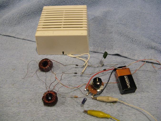 The attitude towards self-assembled devices today is somewhat negative, and the expression "assemble on the knee" is overly negative. But let's not listen to envious people, but immediately turn to the first stage.
 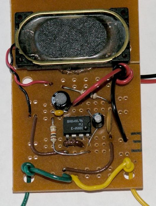 First you need to choose a scheme. Homemade ULF type can be made on transistors or a microcircuit. The first option is highly discouraged for beginner radio amateurs, as they will clutter up the board, and the repair of the device will become more complicated. It is best to replace a dozen transistors with one monolithic microcircuit. Such a homemade amplifier will delight the eye, it will turn out to be compact, and it will take a little time to assemble it.
To date, the most popular and reliable chip is the TDA2005 type. It is already in itself a two-channel ULF, it is enough just to organize power supply and apply input and output signals. Such a simple homemade amplifier will cost no more than a hundred rubles, along with other parts and wires.
The output power of the TDA2005 ranges from 2 to 6 watts. This is enough for listening to music at home. The list of parts used, their parameters and, in fact, the circuit itself is shown below.
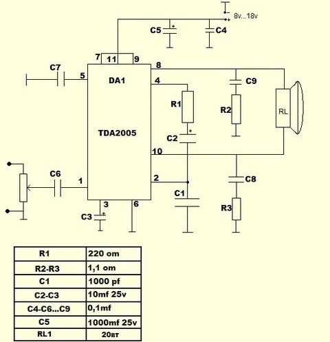 When the device is assembled, it is recommended to screw a small aluminum screen to the microcircuit. Thus, when heated, heat will be better dissipated.
Such a homemade amplifier is powered by 12 volts. To implement it, a small power supply or an electrical adapter is purchased with the ability to switch the output voltage values. The current of the device is not more than 2 amperes.
Speakers up to 100 watts can be connected to such an ULF amplifier. The amplifier can be input from a mobile phone, DVD player or computer. At the output, the signal is taken through a standard headphone jack.
Thus, we figured out how to assemble an amplifier in a short time for little money. Rational Decision practical people!
Amplifying block of an amateur radio complex
Main specifications power amplifier:
Rated output power, W, ....................2x25 (2x60)
Power band, kHz .............................................. 0.02 ...150(100)
Rated input voltage, V............................................... 1(1)
Harmonic coefficient, %, at frequency, kHz:
1 .............................................................................. 0,1(0,1)
2 ............................................................................ 0,14(0,55)
10 ............................................................................ 0,2(0,9)
20 ............................................................................. 0,35(1,58)
Intermodulation distortion factor, %,......... 0.3(0.47)
Input impedance, kOhm .............................................. .150
Quiescent current of the output stage, mA .......................................... 50 (50 )
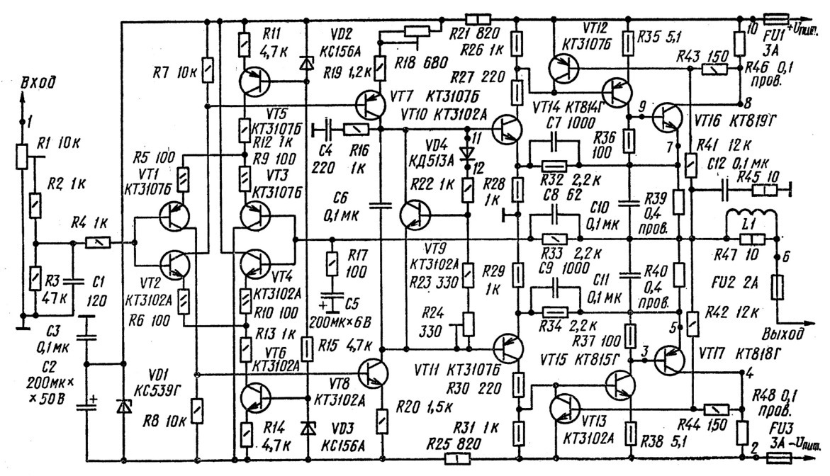
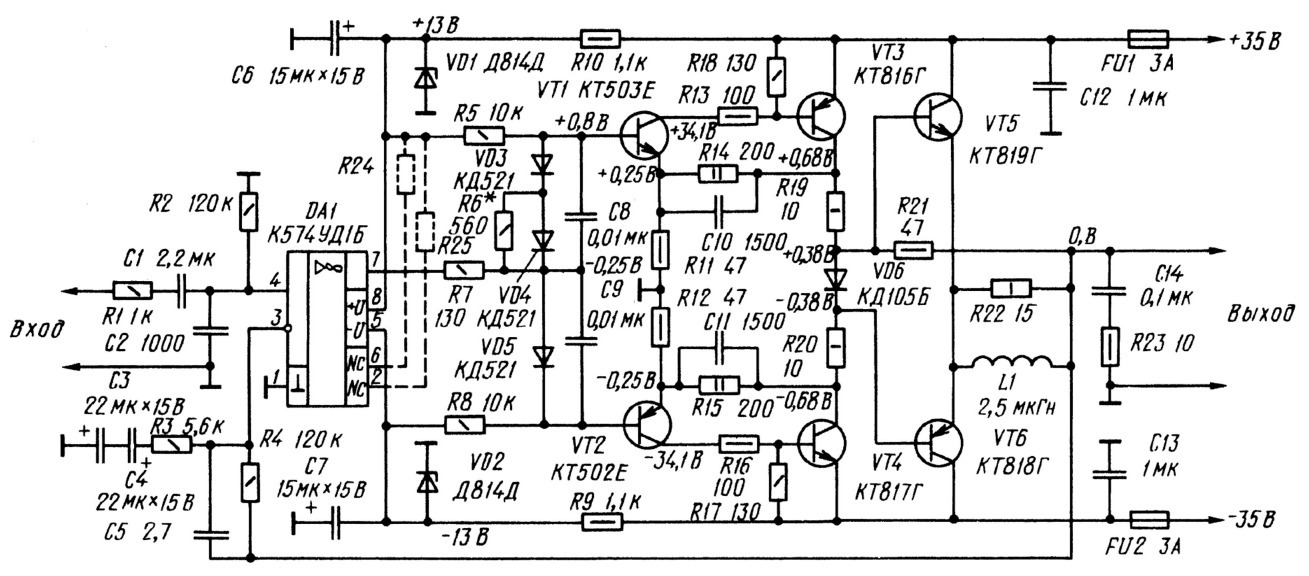
The signal voltage amplification cascade is made on the OU A1. As can be seen from the diagram, part of the output signal is supplied to its power circuit through the R6C3C4R4R5 circuit (together with the zener diodes V6, V7, the elements of this circuit, except for the resistor R6, provide stabilization and filtering of the supply voltages). As a result, the voltage at the power supply terminals of the op-amp at the maximum signal is shifted (relative to the common wire) in the corresponding direction and the range of the output signal of the op-amp increases significantly. The large common-mode signals that arise at the inputs of the op-amp are not dangerous, since the op-amp suppresses them well (typical value of the attenuation coefficient is 70 ... 90 dB). When a signal is applied to the inverting input, the stabilized supply voltages should not exceed + -28 V, on the inverting ones - a value equal to (11in + 28 V), where 11in is the amplitude of the input signal. The unused input must in any case be connected to a common wire. OA K140UD8A in power amplifiers can be replaced by K140UD8B, K140UD6, K140UD10, K140UD11, K544UD1. The worst results are given by the use of OU K140UD7. It is not at all recommended to use OU K140UD1B, K140UD2A, K140UD2B, K153UD1. Instead of KS518A zener diodes, you can use D814A, D814B zener diodes connected in series with a total stabilization voltage of about 18V.
High quality ULF
The amplifier described below is suitable for amplifying high-power audio signals in high-end audio applications, as well as for use as a high-power broadband operational amplifier.
The main technical characteristics of the amplifier:
Rated output power, W, with load resistance,
Ohm: 8 ............................................... ...............................................48
4..........................................................................................60
The range of reproducible frequencies with a frequency response unevenness of not more than 0.5 dB and an output power of 2 W, Hz..................................10...200000
THD at rated power
in the range of 20...20000 Hz, %........................................ ............0.05
Rated input voltage, V .............................................. 0.8
Input impedance, kOhm .............................................. ........47
Output impedance, Ohm .............................................. ....0.02
The input stage of the amplifier consists of two differential amplifiers (connected in parallel) made on transistors VT1, VT3 and VT2, VT4 of the opposite structure. Current generators on transistors VT5, VT6 provide stability of values (about 1 mA) of total emitter currents of differential pairs, as well as decoupling in power circuits. The signal to the output amplifier is supplied from controlled current generators (VT7, VT7), which operate in antiphase. Such an inclusion doubled the "buildup" current, reduced non-linear distortion and improved the frequency properties of the amplifier as a whole. Each of the arms of the symmetrical output amplifier is made according to the Darlington circuit, and is a three-stage amplifier (in two stages, transistors are connected according to a common emitter circuit and in one - with a common collector). The amplifier is covered by a frequency-dependent OOS, which determines its voltage transfer coefficient, which is close to three in the audio range. Since the feedback signal taken from the resistor R39 (R40) is proportional to the changes in the current of the output transistor, a rather rigid stabilization of the operating point of this transistor is additionally carried out. The bias voltage of the output stage is determined by the resistance of the collector-emitter junction of the transistor VT9 and is regulated by resistor R24. The bias voltage is thermally stabilized by the VD4 diode, which is mounted on the heat sink of one of the powerful transistors.
Correction elements R16, C4, C6 - C11 ensure the stability of the amplifier and equalize its frequency response. Passive filter low frequencies R2C1 prevents RF signals from entering the input. Chain C12R45L1R47 compensates for the reactive component of the load resistance. On transistors VT12 and VT13, a unit for protecting output transistors from current and voltage overloads is assembled. Resistor R1 allows, if necessary, to limit the output power in accordance with the signal level from the preamplifier and the capabilities of the speaker used.
Other low-power high-frequency silicon transistors can also be used in the amplifier, for example, KT342A, KT342B and KT313B, KT315 and KT361 (with indices from B to E). Transistors VT14 and VT15 (possible replacement - KT816V, KT816G and KT817V, KT817G or KT626V and KT904A) are equipped with ribbed heat sinks with dimensions of 23x25x12 mm. As output transistors, you can use the KT818GM and KT819GM transistors, which allow you to get power over 70 W when the supply voltage increases. Zener diode VD1 can also be D816G or 2S536A, VD2 and VD3 - KS147A (with appropriate correction of the resistances of resistors R11 and R14).
AF power amplifier
Rated (maximum) power, W...................... 60(80)
Nominal frequency range, Hz.................................. 20...20000
Harmonic coefficient in the nominal frequency range, % 0.03
Rated input voltage, V .............................................0.775
Output impedance, Ohm, not more than .............................. 0.08
Output voltage slew rate, V/µs............... 40
The main voltage gain provides a cascade on a high-speed op-amp DA1. The final stage of the amplifier is assembled on transistors VT1 - VT4. Unlike the prototype, the described amplifier has an output emitter follower, made on transistors VT5, VT6, operating in the "B" mode. Temperature stability is achieved by including resistors in the collector circuits VT3, VT4 relatively more resistance R19, R20. Each arm of the pre-terminal stage is covered by a local OOS circuit with a depth of at least 20 dB. The OOS voltage is removed from the collector loads of transistors VT3, VT4 and is fed through dividers R11R14 and R12R15 to the emitter circuits of transistors VT1, VT2. Frequency correction and stability in the OOS circuit is provided by capacitors SYU, C11. Resistors R13, R16 and R19, R20 limit the maximum currents of the pre-terminal and final stages of the amplifier during a short circuit of the load. In case of any overloads, the maximum current of transistors VT5, VT6 does not exceed 3.5 ... 4 A, and in this case they do not overheat, since the fuses FU1 and FU2 have time to burn out and turn off the power to the amplifier.
The harmonic reduction was achieved by introducing a deep (at least 70 dB) general OOS, the voltage of which is taken from the amplifier output and fed through the divider C3C5R3R4 to the inverting input of the op-amp DA1. Capacitor C5 corrects the frequency response of the amplifier through the OOS circuit. The R1C1 circuit included at the input of the amplifier limits its bandwidth to 160 kHz. The maximum possible linearization of AChKhUMZCH in the band 10 ... 200 Hz is achieved by the appropriate choice of the capacitance of capacitors C1, C3, C4.
Instead of those indicated on the diagram, you can use the OU K574UD1A, K574UD1V and transistors of the same types as in the diagram, but with indices G, D (VT1, VT2) and V (VT3 - VT6).
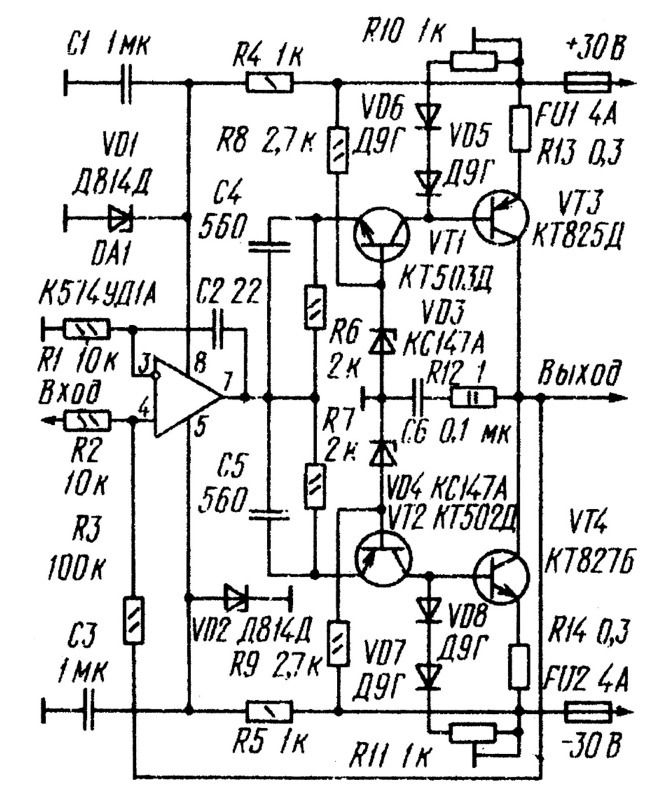
UMZCH with an output stage on field-effect transistors
Main technical characteristics:
Rated (maximum) output power, W.. 45(65)
Harmonic coefficient, %, not more, .............................. 0.01
Rated input voltage, mV .............................. 775
Rated frequency range, Hz, ......................... 20...100000
Output voltage slew rate, V/µs, .................60
Signal-to-noise ratio, dB .............................................. ......... 100
The input stage of the amplifier is made on the op-amp DA1. To increase the amplitude of the output voltage, the output transistors of the UMZCH are controlled by the power supply circuits of the op-amp. The output signal is taken from the positive power terminal DA1 and through the transistor VT1 connected according to the OB circuit is fed to one of the inputs of the differential stage on transistors VT2, VT4. A stabilized voltage is supplied to its second input from a divider formed by diodes VD2 - VD5 and resistor R13.
The described amplifier does not require any special measures to protect the output transistors from short circuits in the load, since the maximum voltage between the source and the gate is only twice the same voltage in idle mode and corresponds to a current through the output transistor of about 9 A. Such a current the applied transistors reliably withstand during the time required to blow the fuses and disconnect the UMZCH from the power source.
Coil L1 is wound in one layer on a toroidal frame with an outer diameter of 20, an inner diameter of 10 and a height of 10 mm and contains 28 turns of PEV-2 1.0 wire.
In UMZCH, it is desirable to use the op-amp KR544UD2A, as the most broadband domestic op-amp with internal frequency correction. Transistors KT3108A are interchangeable KT313A, KT313B, and KP912B - KP912A and KP913, KP920A. 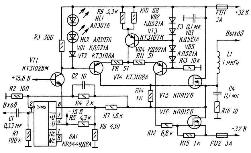
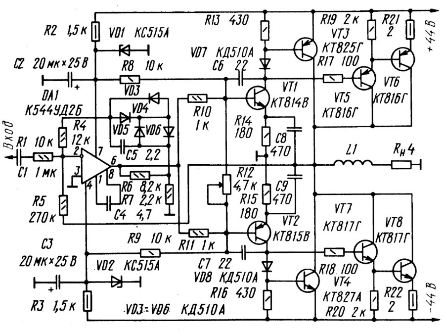
High quality power amplifier
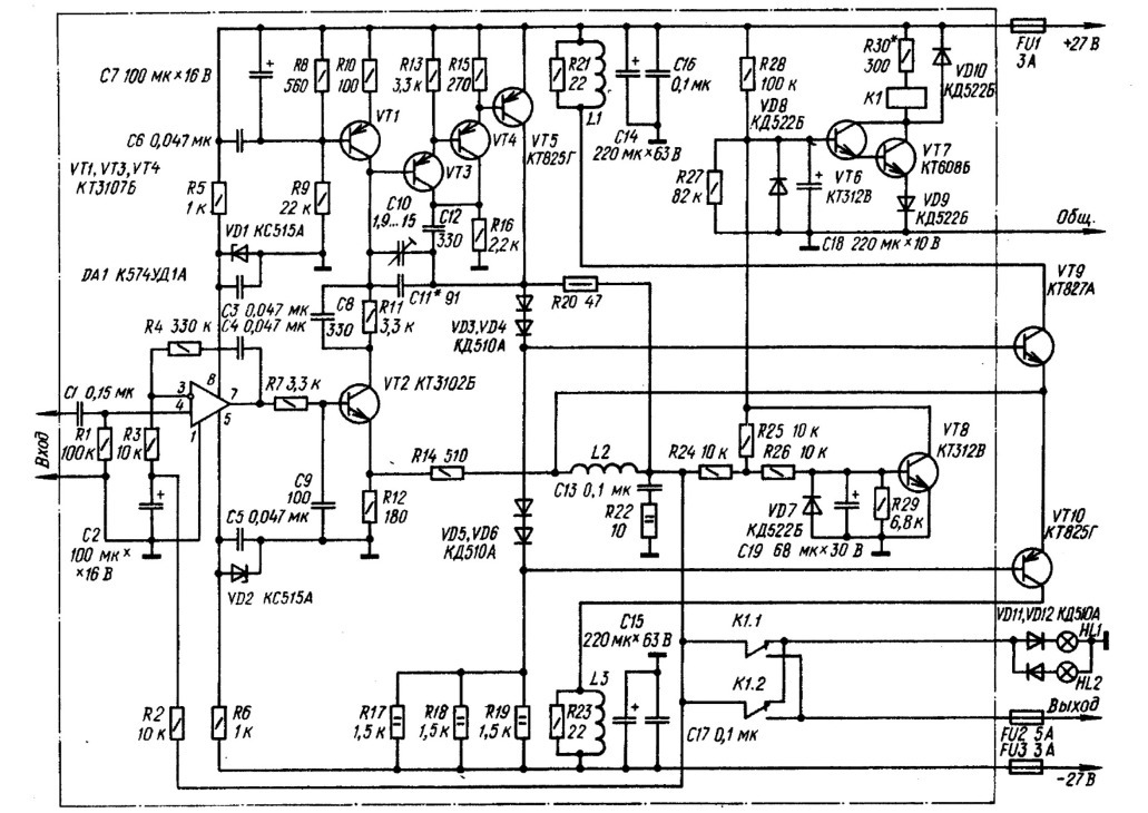
When designing the amplifier described below, the Kvod-405 amplifier was taken as a basis, successfully combining high technical characteristics and circuit simplicity. Structural scheme the amplifier basically remained unchanged, only devices for protecting the transistors of the output stage from overload were excluded. Practice has shown that devices of this kind do not completely exclude transistor failures, but often introduce non-linear distortions at maximum output power. The current of transistors can be limited in other ways, for example, using overcurrent protection in voltage regulators. At the same time, it seems expedient to protect loudspeakers in case of failure of the amplifier or power supplies. To improve the symmetry of the amplifier, the output stage is made on a complementary pair of transistors, and to reduce non-linear distortions of the "step" type, diodes VD5, VD6 are included between the bases of transistors VT9, VT10. This ensures a sufficiently reliable closing of the transistors of the output stage in the absence of a signal. Slightly changed the input circuit. The non-inverting input of the op-amp DA1 was used as a signal, which made it possible to increase the input impedance of the amplifier (it is determined by the resistance of the resistor R1 and is equal to 100 kOhm.) However, it should be noted that in the non-inverting version, the stability of the amplifier remains high. To prevent clicks in the speakers caused by power-on transients, and to protect the speakers from constant voltage in case of failure of the amplifier or power supplies, a simple, well-proven device (VT6 - VT8) used in the industrial amplifier "Brig - 001" was used. When this device is triggered, one of the lamps HL1, HL2 lights up, indicating the presence of a constant voltage of one or another polarity at the output of the amplifier. Basically, the circuit of the described amplifier does not differ from the circuit of the Kvod-405 amplifier. The coils are wound with wire PEV-2 1.0 on frames with a diameter of 10 mm and contain: L1 and L3 - 50 turns each (inductance - 5 ... 7 μH), L2 - 30 turns (3 μH).
Instead of those indicated in the diagram in the amplifier, you can use the OU K574UD1B, K574UD1V, K544UD2, and also (with some deterioration in the parameters) K544UD1 and K140UD8A - K140UD8V; transistors KT312V, KT373A(VT2), KT3107B, KT3107I, KT313B, KT361V, KT361K (VT1, VT3, VT4), KT315V (VT6, VT8), KT801A, KT801B (VT7). Each of the KT825G transistors can be replaced with composite transistors KT814V, KT814G + KT818V, KT818G, and KT827A with composite transistors KT815V, KT815G + KT819V, KT819G. Diodes VD3 - VD6, VD11, VD12 - any silicon diodes with a maximum forward current of at least 100 mA, VD7 - VD10 - the same, but with a maximum current of at least 50 mA. In the absence of KS515A zener diodes, it is permissible to use D814A, D814B or KS175A zener diodes connected in series.
Maximum output power, W, at a load of 4 Ohm..... 2x70
Rated input voltage, V .............................................. 0.2
Upper limit of the frequency range, kHz .............................. 50
Output voltage slew rate, V/µs...............5.5
Signal-to-noise ratio (unweighted), dB............................................... 80
Harmonic coefficient, %, no more than, .................................................0, 05
Amplifier with multi-loop feedback
Main technical characteristics:
Rated frequency range, Hz, ............................... 20...20000
Rated load resistance, Ohm .......................................... 4
Rated (maximum) vy. power, W, with load resistance, Ohm:
4 .................................................................................. 70(100)
8 ........................................................................................40(60)
Frequency range, Hz, .................................... ........ 5...100000
Output voltage slew rate, V/µs, min... 15 Harmonic factor, %, max, at frequency, Hz:
20...5000 .................................................................................. 0,001
10000 ................................................................................ 0,003
20000 ................................................................................. 0,01
Harmonic coefficient, %, no more than, ...................................... 0.01
Rated input voltage, V .......................................... 1
Input impedance, kOhm, not less, ........................................... 47
The first stage is assembled on an operational amplifier (op-amp) DA1, the rest - on transistors (the second and third - respectively on VT1, VT3, the fourth - on VT8, VT11 and VT10, VT12, the fifth - on VT13, VT14). In the fourth (pre-terminal) stage, transistors of different structures were used, connected according to the scheme of a composite emitter follower, which made it possible to introduce local feedback into it and thus increase the linearity and reduce the output resistance. To reduce transient distortion on high frequencies the output stage operates in AB mode, and the resistance of the bias circuit resistors (R30, R33) is limited to 15 ohms. All transistor stages of the amplifier are covered by a local OOS circuit with a depth of at least 50 dB. The OOS voltage is removed from the output of the amplifier and fed through the divider R10R12 to the emitter circuit of the transistor VT1. Frequency correction and stability in the OOS circuit are provided by capacitor C4. The introduction of local OOS made it possible, even with the most unfavorable combinations of amplifying properties of transistors, to limit the harmonic coefficient of this part of the amplifier to 0.2%. The protection device consists of a trigger on transistors VT6, VT7 and a threshold element on the transistor VT9. As soon as the current through any of the output transistors exceeds 8 ... 9 A, the transistor VT9 opens, and its collector current opens the trigger transistors VT6, VT7.
AF power amplifier
The AF amplifier offered to the attention of radio amateurs has very low coefficients of harmonic and intermodulation distortion, it is relatively simple, capable of withstanding short-term short circuit in the load, does not require external elements for thermal stabilization of the current of the transistors of the output stage.
Main technical characteristics:
Max power at a load of 4 ohms, W...................... 80
Rated frequency range, Hz....................................20....20000
Harmonic coefficient at maximum output power 80 W, %, at frequency:
1 kHz.............................................. ................................. 0.002
20..................................................................................... 0,004
The coefficient of intermodulation distortion,%.............0.0015
Output voltage slew rate, V/µs...............................40
To increase the input resistance, transistors VT1, VT2 are introduced into the AF amplifier. This facilitated the work of the op-amp DA1 and made it possible to provide a stable base-emitter voltage of transistors VT3, VT4 when the temperature changes.
Resistor R14 sets the symmetry of the arms of the output stage of the amplifier. 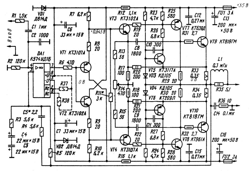
Simple Power Amplifier
Main technical characteristics:
Input voltage, V.............................................. ................1.8
Input impedance, kOhm .............................................. .......10
Rated output power, W, .......................................... 90
Nominal frequency range, Hz.................................... 10...20000
Harmonic coefficient, %, at frequency, Hz:
200 .................................................................................... 0,01
2000 ............................................................................ 0,018
20000 ............................................................................... 0,18
Relative noise level, dB, not more than .............................. -90
Output voltage slew rate, V/µs .................. 17
The power amplifier consists of a voltage amplification stage on a high-speed op-amp DA1 and an output stage on transistors VT1 - VT4. The transistors of the complementary pair of the pre-terminal stage (VT1 - VT2) are connected according to the scheme with a common base, and the final one (VT3 - VT4) - with a common emitter. This inclusion of powerful composite transistors of the final stage provides signal amplification not only in current, but also in voltage. The symmetry of the arms of the output stage helps to reduce the harmonic distortion introduced by the amplifier. For the same purpose, it is covered by a common OOS circuit, the voltage of which is taken from the output of the amplifier and fed through the resistor R3 to the non-inverting input of the op-amp. Capacitors C4, C5, shunt resistors R6, R7 reduce step-type distortion. The R12C6 circuit prevents self-excitation of the amplifier in the region of higher audio frequencies and increases the stability of its operation with a reactive load. The gain depends on the ratio of the resistances of the resistors R2, R3. With the ratings indicated on the diagram, it is equal to 10.
To power the amplifier, any unstabilized bipolar source with a voltage of 25 ... 45 V is suitable. Instead of KT503D transistors, you can use KT503E, instead of KT502D - KT502E. Transistors KT827B and KT825D can be replaced by composite transistors KT817G + KT819GM and KT816G + KT818GM, respectively.
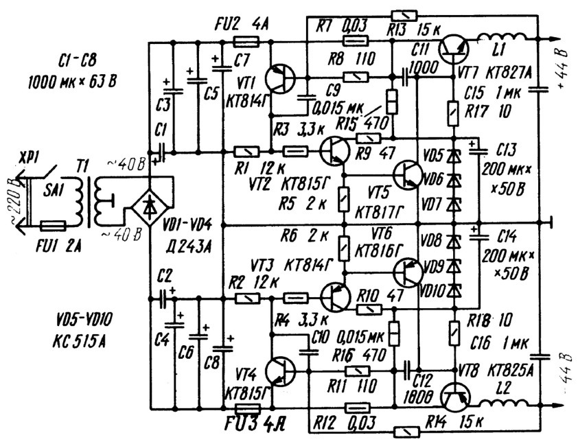
200W power amplifier with power supply
Main technical characteristics:
Rated frequency range, Hz............................... 20...20000
Maximum output power, W, at a load of 4 ohms ........ 200
Harmonic coefficient, %, at output power 0.5..150 W at frequency, kHz
1 ..........................................................................................0,1
10 .................................................................................... 0,15
20 .................................................................................... 0,2
Efficiency, %.................................................. ............................................. 68
Rated input voltage, V .............................................. 1
Input impedance, kOhm .............................................. .. 10
Output voltage slew rate, V/µs .......... 10
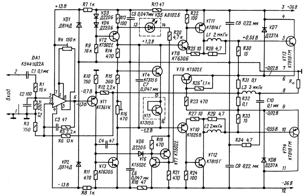
The pre-amplification stage is based on a high-speed op amp DA1 (K544UD2B), which, along with the necessary voltage gain, ensures stable operation of the amplifier with deep feedback. Feedback resistor R5 and resistor R1 determine the gain of the amplifier. The output stage is made on transistors VT1 - VT8. Zener diodes VD1, VD2 stabilize the supply voltage of the op-amp, which is simultaneously used to create required voltage output stage bias. Capacitors C4, C5 are corrective. With an increase in the capacitance of the capacitor C5, the stability of the amplifier increases, but at the same time, non-linear distortions increase, especially at higher audio frequencies. The amplifier remains operational when the supply voltage drops to 25 V.
As a power source, you can use a conventional bipolar power supply, circuit diagram which Powerful composite transistors VT7 and VT8, connected according to the emitter follower circuit, provide fairly good filtering of supply voltage ripples with the mains frequency and stabilization of the output voltage thanks to the zener diodes VD5 - VD10 installed in the base circuit of the transistors. Elements L1, L2, R16, R17, C11, C12 eliminate the possibility of high-frequency generation. Resistors R7, R12 of the power supply are a segment copper wire PEL, PEV-1 or PELSHO with a diameter of 0.33 and a length of 150 mm, wound on the body of the MLT-1 resistor. The power transformer is made on a toroidal magnetic core made of E320 electrical steel, 0.35 mm thick, tape width 40 mm, inner diameter of the magnetic core 80, outer diameter 130 mm. The network winding contains 700 turns of PELSHO 0.47 wire, the secondary - 2x130 turns of PELSHO 1.2 mm wire.
Instead of OU K544UD2B, you can use K544UD2A, K140UD11 or K574UD1. Each of the KT825G transistors can be replaced by composite transistors KT814G, KT818G, and KT827A by composite transistors KT815G, KT819G. Diodes VD3 - VD6 UMZCH can be replaced by any high-frequency silicon diodes, VD7, VD8 - by any silicon diodes with a maximum forward current of at least 100 mA. Instead of KS515A zener diodes, you can use D814A (B, C, G, D) and KS512A zener diodes connected in series.
BP
After mastering the basics of electronics, a novice radio amateur is ready to solder his first electronic designs. Audio power amplifiers tend to be the most repeatable designs. There are a lot of schemes, each differs in its parameters and design. This article will look at some of the simplest and most fully working amplifier circuits that can be successfully repeated by any radio amateur. Not used in the article complex terms and calculations, everything is simplified as much as possible so that there are no additional questions.
Let's start with a more powerful scheme.
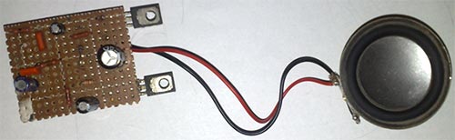
So, the first circuit is made on the well-known TDA2003 chip. This is a mono amplifier with an output power of up to 7 watts into a 4 ohm load. I want to say that standard scheme The inclusion of this microcircuit contains a small number of components, but a couple of years ago I came up with a different circuit on this microcircuit. In this scheme, the number of components is minimized, but the amplifier has not lost its sound parameters. After the development of this circuit, I began to make all my amplifiers for low-power speakers on this circuit.
The circuit of the presented amplifier has a wide range of reproducible frequencies, the supply voltage range is from 4.5 to 18 volts (typical 12-14 volts). The microcircuit is installed on a small heat sink, since the maximum power reaches up to 10 watts.
The microcircuit is capable of operating at a load of 2 ohms, which means that 2 heads with a resistance of 4 ohms can be connected to the amplifier output.
The input capacitor can be replaced with any other, with a capacity of 0.01 to 4.7 uF (preferably from 0.1 to 0.47 uF), you can use both film and ceramic capacitors. All other components should not be replaced.
Volume control from 10 to 47 kOhm.
The output power of the microcircuit allows it to be used in low-power PC speakers. It is very convenient to use a chip for stand-alone speakers for a mobile phone, etc.
The amplifier works immediately after switching on, it does not need additional adjustment. It is advised to additionally connect the minus power supply to the heat sink. All electrolytic capacitors are preferably used at 25 volts.
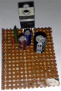
The second circuit is assembled on low-power transistors, and is more suitable as a headphone amplifier.
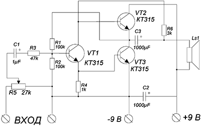
This is probably the highest quality circuit of its kind, the sound is clear, the entire frequency spectrum is felt. With good headphones, it feels like you have a full subwoofer.
The amplifier is assembled on only 3 reverse conduction transistors, as the cheapest option, transistors of the KT315 series were used, but their choice is quite wide.
The amplifier can operate on a low-impedance load, up to 4 ohms, which makes it possible to use the circuit to amplify the signal of a player, radio receiver, etc. A 9 volt battery was used as a power source.
KT315 transistors are also used in the final stage. To increase the output power, you can use KT815 transistors, but then you will have to increase the supply voltage to 12 volts. In this case, the power of the amplifier will reach up to 1 watt. The output capacitor can have a capacitance from 220 to 2200 uF.
The transistors in this circuit do not heat up, therefore, no cooling is needed. When using more powerful output transistors, you may need small heatsinks for each transistor.
And finally - the third scheme. A no less simple, but proven version of the amplifier structure is presented. The amplifier is capable of operating undervoltage up to 5 volts, in this case, the output power of the PA will be no more than 0.5 W, and the maximum power when powered by 12 volts reaches up to 2 watts.
The output stage of the amplifier is built on a domestic complementary pair. Adjust the amplifier by selecting the resistor R2. To do this, it is desirable to use a 1 kOhm trimmer. Slowly rotate the knob until the quiescent current of the output stage is 2-5 mA.
The amplifier does not have a high input sensitivity, so it is advisable to use a preamplifier before the input.
A diode plays an important role in the circuit; it is here to stabilize the output stage mode.
The output stage transistors can be replaced with any complementary pair of appropriate parameters, for example, KT816/817. The amplifier can power low-power autonomous speakers with a load resistance of 6-8 ohms.
A low frequency amplifier (ULF) is such a device for amplifying electrical vibrations corresponding to the frequency range audible to the human ear, i.e. ULF should amplify in the frequency range from 20 Hz to 20 kHz, but some ULF can have a range up to 200 kHz. ULF can be assembled as an independent device, or used in more complex devices - TVs, radios, radios, etc.
The peculiarity of this circuit is that the 11th output of the TDA1552 microcircuit controls the operating modes - Normal or MUTE.
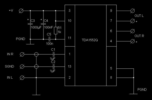
C1, C2 - bypass blocking capacitors, used to cut off the constant component of the sinusoidal signal. Electrolytic capacitors should not be used. It is desirable to place the TDA1552 chip on a heatsink using heat-conducting paste.
In principle, the presented circuits are bridge circuits, since there are 4 amplification channels in one TDA1558Q microassembly case, therefore pins 1 - 2, and 16 - 17 are connected in pairs, and they receive input signals from both channels through capacitors C1 and C2. But if you need an amplifier for four speakers, then you can use the circuit option below, although the power will be 2 times less per channel.
The basis of the design is the TDA1560Q class H microassembly. The maximum power of such a ULF reaches 40 W, with a load of 8 ohms. Such power is provided by an approximately doubled voltage due to the operation of the capacitors.

The output power of the amplifier in the first circuit assembled on the TDA2030 is 60W at a load of 4 ohms and 80W at a load of 2 ohms; TDA2030A 80W at 4 ohm load and 120W at 2 ohm load. The second circuit of the considered ULF is already with an output power of 14 watts.

This is a typical two-channel ULF. With a little piping of passive radio components on this chip, you can assemble an excellent stereo amplifier with an output power of 1 watt per channel.
Microassembly TDA7265 - is a fairly powerful two-channel Hi-Fi class AB amplifier in a typical Multiwatt package, the microcircuit has found its niche in high-quality stereo technology, Hi-Fi class. Simple switching circuits and excellent parameters made the TDA7265 a perfectly balanced and excellent solution for building high-quality amateur radio equipment.
The Micro Assembly is a class AB quad amplifier designed specifically for use in automotive audio applications. Based on this microcircuit, several high-quality ULF variants can be built using a minimum of radio components. The microcircuit can be advised to beginner radio amateurs for home assembly of various acoustic systems.
The main advantage of the amplifier circuit on this microassembly is the presence of four independent channels in it. This power amplifier works in AB mode. It can be used to amplify various stereo signals. If desired, you can connect to the speaker system of a car or a personal computer.
TDA8560Q is just a more powerful analogue of the TDA1557Q chip, widely known to radio amateurs. The developers only strengthened the output stage, thanks to which the ULF is perfect for a two-ohm load.
The LM386 micro-assembly is a ready-made power amplifier that can be used in low-voltage designs. For example, when the circuit is powered by a battery. LM386 has a voltage gain of about 20. But by connecting external resistances and capacitances, you can adjust the gain up to 200, and the output voltage automatically becomes equal to half the supply voltage.
The LM3886 micro-assembly is a high quality amplifier with an output of 68 watts into 4 ohms or 50 watts into 8 ohms. At the peak moment, the output power can reach a value of 135 watts. A wide voltage range from 20 to 94 volts is applicable to the microcircuit. Moreover, you can use both bipolar and unipolar power supplies. The ULF harmonic coefficient is 0.03%. Moreover, this is over the entire frequency range from 20 to 20,000 Hz.
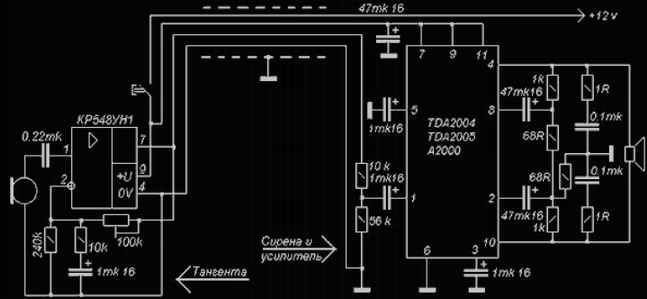
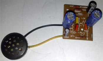
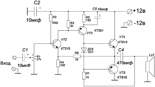
The circuit uses two ICs in a typical connection - KR548UH1 as a microphone amplifier (installed in the PTT) and (TDA2005) in bridge connection as a terminal amplifier (installed in the siren case instead of the original board). As an acoustic emitter, a modified alarm sipen with a magnetic head is used (piezo emitters are not suitable). Improvement consists in disassembling the siren and throwing out the native tweeter with an amplifier. Microphone - electrodynamic. When using an electret microphone (for example, from Chinese handsets), the connection point of the microphone with the capacitor must be connected to + 12V through a resistor ~ 4.7K (after the button!). The 100K resistor in the K548UH1 feedback circuit is better to put with a resistance of ~ 30-47K. This resistor is used to adjust the volume. It is better to install the TDA2004 chip on a small radiator.
To test and operate - with a radiator under the hood, and a tangent in the cabin. Otherwise, squealing due to self-excitation is inevitable. The trimmer resistor sets the volume level so that there is no strong sound distortion and self-excitation. With insufficient volume (for example, a bad microphone) and a clear margin of power of the emitter, you can increase the gain of the microphone amplifier by increasing the value of the trimmer in the feedback circuit several times (the one that is 100K according to the scheme). In a good way - we would need another primambas that does not allow the circuit to self-excite - some kind of phase-shifting chain or a filter for the excitation frequency. Although the scheme and without complications works fine
We advise you to read
 Therapeutic effect What is vitamin e used for?
 - instructions for use Dexalgin how to take") Dexalgin (ampoules with dexketoprofen) - instructions for use Dexalgin how to take
Dexalgin (ampoules with dexketoprofen) - instructions for use Dexalgin how to take Diclak solution - instructions for use Diclofenac injections instructions for use for children
 Dream Interpretation: why dream of Fire, to see Fire in a dream, which means Why dream of fire in a mirror

