] >>> The radio receiver "Ocean-205" is a further modification of the receivers "Ocean" and "Ocean-203" considered in § 3. circuit diagram it is given in Fig. 19 (inset), however, it does not show the RF-IF block diagram, since it practically does not differ from the corresponding circuit of the Okean-203 receiver (minor changes are specified below). For the board of the RF-IF unit, the diagram shows only contacts for connecting external circuits.
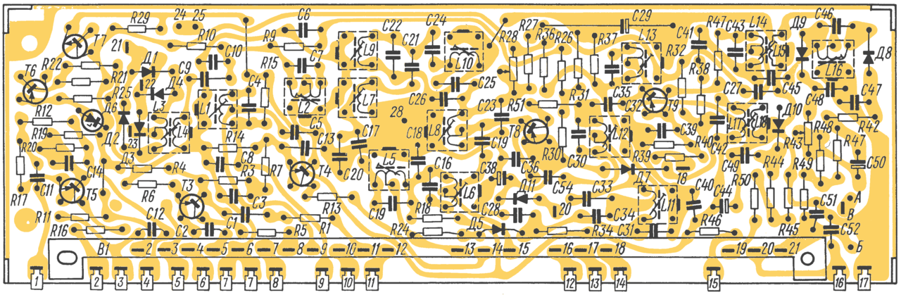
Rice. 19. Schematic diagram of the radio receiver "Ocean-205"
Range switch B - in position KBV ( P1), AM-FM switch ( B1) - in position AM (VHF off), other switches IN 2-AT 5- in off state. Magnetic Antenna ( MA) is connected to the switch position AT: CB range - to contacts 15
, 17
slats P6, DV - 14
, 19
slats P7. Schemes of slats P1, P2 and P3, P4 combined, in parentheses are the ratings of the elements of the bars P2 and P4(other denominations have no differences)
Telescopic antenna signal through coupling capacitor C8 goes to the coupling coil L1. To ensure the highest gain and lowest noise level, the wideband input circuit ( L2, C1, C2) is made non-configurable and has an inductive connection with the antenna. The contour stripe width is ~ 7.5 MHz with its constant setting to the middle of the range (69.5 MHz). Connection of the input circuit with the emitter T1(UHF) - capacitive (capacitor divider C1 and C2), which makes setting up the circuit more convenient.
UHF transistor ( T1) is connected according to the common base scheme, since such inclusion does not require neutralization and provides more uniform gain over the range. The UHF cascade has an output >>> single resonant circuit L3, C4, C6, C7 with autotransformer. Tuning it to the received frequency is associated with tuning the local oscillator circuit and is carried out by a two-section KPI block of variable capacitors ( C7 and C21). Resistor R12 is antiparasitic. The load of the UHF circuit is the input impedance of the frequency converter, and the connection of this circuit with the transistor T2 carried out through a small capacitor C8. To reduce stage overloads and local oscillator detuning with strong input signals, a clamping diode is connected in parallel with the UHF circuit. D12 (D20), to which the blocking voltage from the stabilizer is applied.
The load of the converter is an IF bandpass filter, consisting of two coupled circuits ( L5, C14 and L6, C18). The required bandwidth is provided by the amount of coupling between the loops. With additional winding L7, inductively coupled to the coil L6, the matching of the output impedance of the frequency converter with the input impedance of the IF path is achieved.
Varicap is used for automatic frequency control. D13(D902), which is connected to the local oscillator circuit through capacitors C19 and C20. The control voltage to the varicap is supplied from the frequency detector through a resistor R52(installed between points BUT and B RF-IF boards, see fig. 17) and contact 27 (dot AT fees); contact 6 and resistor R10(VHF unit). This voltage acts on the varicap so that the frequency difference between the local oscillator and the received signal approaches nominal value intermediate frequency due to the fact that the capacitance of the varicap changes with a change in the blocking voltage, and hence the frequency of the local oscillator.
Rice. 17. Wiring diagram of the RF-IF board of the Ocean-203 radio receiver
The diagram does not show transistor shields. T3, T4, T5, T8 and T9 and the position of the movable switch blades IN 1
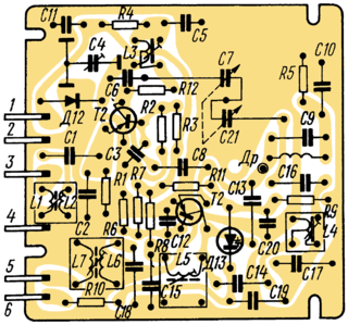
Rice. 20. Wiring diagram of the board of the VHF radio receiver "Ocean-205"
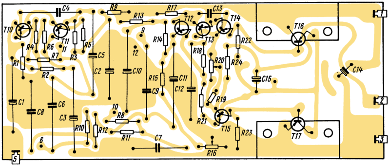
Rice. 21. Wiring diagram of the board of the ULF radio receiver "Ocean-205"
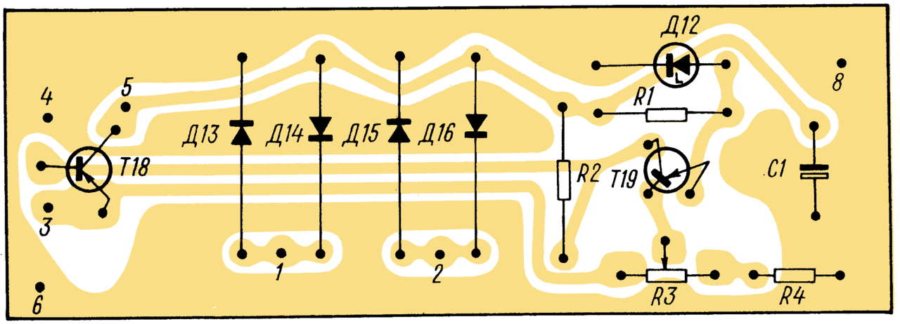
Rice. 22. Wiring diagram of the rectifier board of the radio receiver "Ocean-205"
The ULF receiver circuit is somewhat different from that considered in § 3. The first two pre-amplification stages and the four-transistor ULF output stage practically do not differ in their circuits from those considered in § 3. In the one shown in fig. 19 (see insert) the bass amplifier circuit has changed the connection of the tone controls for high ( R3) and low ( R2) to sound frequencies. The scheme of their inclusion is similar to that used in tube receivers. The entire amplifier is covered by deep negative DC and AC feedback to ensure high mode stability and low harmonic distortion.
Negative constant DC coupling is carried out from the ULF output to the emitter of the transistor T12 through a resistor R21. Positive feedback from the output through a resistor R24 applied to the bases of the transistors T14, T15(phase inverter). With help variable resistor R20 the initial bias is set at the bases of these transistors and thereby the required value of the quiescent current of the output stage is selected. To reduce non-linear distortions, feedback is introduced according to alternating current- chain R18, C12. The necessary blockage of the frequency response is carried out by the feedback capacitor C13 connected between the base and collector of the transistor T13(type KT315B). Transistor base bias T12 set by variable resistor R16. Chain R13, C10 acts as a filter
The wiring diagram of the bass amplifier is shown in fig. 21 (inset).
To power the receiver from a 127/220 V AC mains, a power rectifier was introduced into its composition, made according to a bridge circuit with four diodes D14-D17(D226), and a voltage stabilizer assembled according to a compensation scheme with a single-stage feedback amplifier. On a transistor T19(MP39) the cascade works in amplifier mode direct current, and on T18(P213A) - control cascade. The feedback voltage is applied to the base of the transistor T19 with potentiometer R3, which is part of the divisor ( R3, R4) connected in parallel with the load.
With increasing voltage at the output (contacts 3 , 4 boards) the base current increases T19, and with it the current of its collector. This results in an increase in the voltage drop across the resistor. R2 and decrease the base current T18, which in turn increases the resistance between emitter and collector T18 and, accordingly, the voltage in the same area. As a result, the increase in output voltage is largely compensated. Using a variable resistor R3, you can change the voltage across the load >>> almost from zero value to the value of the reference voltage of the zener diode D18(D814A). The stabilized voltage is removed from the emitter T18 and via switch contacts AT 3(“Network”) and AT 4("On") is fed into the receiver circuitry. Capacitor C1 reduces the ripple of the rectified voltage. Rectifier unit PCB wiring diagram ( Вn) is shown in Fig. 22 (inset).
The receiver power switch is removed from the volume control potentiometer ( R1) to a special switch AT 4. With switch AT 5 the illumination of the scale is turned on and off (Fig. 23 on the insert).

Broadcasting receiver "Ocean-214".
The radio receiver of the 2nd group of complexity with universal power supply “Ocean-214” contains a chassis with printed circuit boards and main blocks and assemblies. The receiver is structurally made according to the functional-block principle. On the front and rear panels there are controls, jacks for connecting an external antenna, tape recorder, headphones. The receiver provides LW, MW, five extended HF sub-bands and a VHF band. Power is supplied from elements of type 373 with a total voltage of 9 V or from the mains through a rectifier.
1. VHF unit [A1]
In principle wiring diagram radio receiver "Ocean-214" (Fig. 1) used a unified unit type VHF-2-1C [A1].
The signal from the telescopic whip antenna WA1 (points 20, 21 on the board [A3]) is fed through the coupling capacitor C1 and the coupling coil L1 to the input circuit L2, C2, C3, which provides the initial suppression of the mirror channel and the forward channel. The input circuit is not tunable, therefore it is made broadband with a bandwidth of 2∆f 0.7, covering the entire VHF range from 65 to 108 MHz.
The input signal from the capacitive divider C2, SZ is fed to the input of the URC, assembled on the transistor V1 according to the common base circuit. Turning on with OB due to 100% OOS improves the characteristics of the cascade at high carrier frequencies of the VHF range, and the high output resistance of the transistor does not bypass the load circuit and does not reduce its quality factor. The URC load is the oscillatory circuit L3, C9, tuned to the frequency of the received signal by a variable capacitor C9. Capacitors C7 and C8 ensure that the tuning limits are within the standard limits of the VHF range. Resistors R1, R2, R4 determine the operating mode of the transistor for direct current.
Fig.1 VHF unit.
The frequency converter uses two transistors - VT3 (mixer) and TV4 (local oscillator). The local oscillator driver circuit consists of an L4 coil, a capacitor C19 and coupling capacitors C18, C22, C23. To auto-tune the frequency of the local oscillator, the V4 varicap is used, the control (blocking) voltage of the APCG is applied to the varicap through the resistor R14 from the output of the fractional detector in the URF-IF unit.
The local oscillator is fed through the decoupling filter R11, C17 from a separate stabilizer with a voltage of + 4.2V. Resistors R6, R8, R10 determine the mode of the transistor V2 for direct current, and capacitor C10 eliminates the OOS for alternating current. Since the transistor V2 is connected according to the circuit with OB due to C13, the mandatory PIC is formed by the capacitor C12 from the collector to the emitter. Oscillations of the local oscillator through the isolation capacitor C15 are fed to the base of the mixing transistor V3 along with the signal of the receiving station through its isolation capacitor C11 ..
The operation mode of the mixer V3 is set by standard piping elements R9, R7, R12, C16 and R13, C21. The load of the mixer is a band-pass double-loop filter (FSS) L5, C20 and L6, C24, tuned to an intermediate frequency of the FM path - 10.7 MHz. It provides selectivity for the adjacent channel.
The intermediate frequency signal from the coupling coil L7 is fed to the base of the transistor VT6 of the URF-IF unit.
2. Block KSDV [A2]
The KSDV [A2] unit consists of a drum range switch with a set of printed circuit boards (slats 7 pcs) and a magnetic antenna WA2 (Fig. 2).
On the drum switch boards, sets of replaceable coils and capacitors are installed, related to the input circuits (on the left in the diagram), the RF amplifier (in the middle) and the local oscillator (on the right). The board is connected to the circuit using 20 pads.
For example, consider the bars of the SV and KV-5 bands, for the rest of the bands the differences are insignificant.
The MW-band input circuit is formed by a variable capacitor section C1.1 and an inductance coil L1 located on the ferrite rod of a magnetic antenna, and the coil L3 is short-circuited. In the LW range, the inductance of the input circuit is the sum of the series-connected coils L1 and L3. From the coupling coil L2 of the magnetic antenna, the signal through the contact group of the range switch (cont. 13.15) and the separating capacitor C9 is fed to the base of the transistor V8 - the AM tract URF.
middle group elements on the SV-bar forms a load tunable URF resonant circuit, which provides selectivity for side reception channels (mirror and direct transmission). It includes the second section of KPE C1.2 and the inductance of the coil L9.1. The trimmer capacitor C12 serves to lay the tunable circuit within the standard boundaries of the CB range. From the L9.2 coupling coil with a midpoint, the signal of the received station is fed to a balanced diode ring mixer V1 ... V4 [A3].
The right group of elements on the SV-bar forms the driving circuit of the local oscillator of the AM path on the transistor V9 [A3]. It consists of the third section KPI C1.3, coil inductance L10.2 and coupling capacitors C13, C14, C15. Resistors R4 and R5 select the required local oscillator mode for stable generation. From the coupling coil L10.1, the local oscillator signal is fed to a balanced diode mixer V1 ... V4 [A3].
The switch strips of the HF bands differ from the MW band only in the input circuits. For example, in KV-5, the input circuit is formed by the inductance of the coil L11.1 and the first section of the KPI C1.1. Capacitors C16, C17 are used to lay the input circuit in the standard range limits. From the coupling coil L11.2, the signal is fed to the base of the transistor V8 - the URF of the AM path [A3].
In the HF bands, the input circuits, consisting of single circuits, have an autotransformer connection with the WA1 telescopic antenna through pin 16.
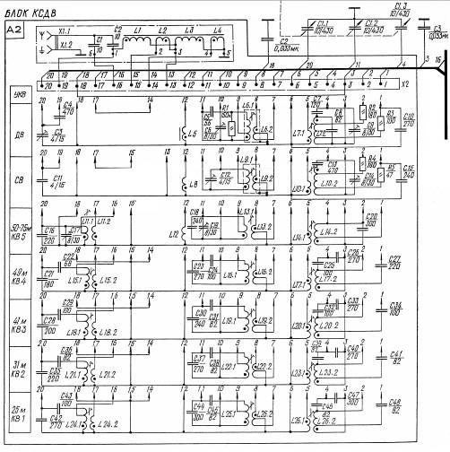
Fig.2 Block KSDV
3. Block URCH - IF [A3]
The URCH-IF block includes the URCH of the AM path, the IF of the AM and FM paths, the frequency converter, the AM and FM detectors, and the voltage stabilizer to power the base circuits of the AM local oscillator.
The URF of the AM path is assembled on a V8 transistor according to a resonant circuit. To increase the stability of its operation, low-resistance resistors R11, R14 are included in the base and collector circuits of the V8 transistor. In the emitter circuit in the ranges DV, SV, KV-5, a filter is included, consisting of a capacitor C14 and the corresponding coil L5, L8, or L12 [A2]. This makes it possible to reduce the uneven amplification of the URF over the range, and also increases the selectivity for side reception channels. A single tunable circuit is connected to the collector circuit of the transistor V8 through the conductor 9 of the bundle located on [A2].
The frequency converter is assembled according to the scheme with a separate local oscillator. The mixer is made on diodes V1...V4 according to a balanced ring circuit. It has a symmetrical input for the signal: the resonant load circuits of the URF located on [A2] through points 7-6 of the board [A3] are connected to the horizontal diagonal of the bridge on diodes V1 ... V4. A circuit L2.2, C7, C8 is connected to the vertical diagonal of the bridge through the coupling coil L2.1 with a midpoint, tuned to an intermediate frequency of the AM signal of 465 kHz. The local oscillator signal is fed to the midpoints of the coupling coils connected to the mixer bridge diagonals L2.1 and L9.2 (for example, for the MW band in the module).
The conductivity of the diodes changes in time with the local oscillator frequency, as a result of which the frequency components of the difference frequency appear at the mixer output:
f pr \u003d f g - f with
The local oscillator is made on the V9 transistor according to the inductive three-point circuit. Capacitor C35 provides the inclusion of a transistor with ABOUT for alternating current. Resistors R24, R25, R22 set the DC mode, and low-resistance R20, R21 increase the stability of the cascade. The local oscillator circuit is included in the POS circuit between the collector and emitters.
The IF circuit with a balanced ring diode mixer is described in detail in the abstract T.5.3.
UFC-AM consists of three stages and is assembled on transistors V7, V10, V15. The load of the first stage is a five-link FSS: L4, C11; L6, C17; L8, C22; L10,C28; L11,SZZ,S34. The connection between the links is critical - through capacitors C16, C20, C25, C29.
The FSS is tuned to an intermediate frequency of 465 kHz, has a bandwidth of 9 kHz, and provides full adjacent channel selectivity.
The load of the second stage is resistor (R31), the third stage is resonant (oscillatory circuit L14, C48).
The amplified 465 kHz intermediate frequency signal is fed to the AM detector, made in series on the V19 diode, and the detector filter C50, R47, R48, C51 to suppress the carrier frequency f pr, After detection, the audio frequency signal c C51 is fed to the input of the audio frequency amplifier UZCH (block [A4]).
The receiver has automatic gain control. AGC. From the collector of transistor V15, through a frequency-dependent circuit R41, C46 and a decoupling capacitor C45, voltage is applied to diode V17, which, together with load resistor R42, forms a parallel-type AGC detector. A DC amplifier is made on the transistor V16, which increases the efficiency of regulation. As the signal grows, the voltage detected by the AGC detector increases and the transistor V16 opens, which leads to a decrease in the voltage on its collector with respect to the emitter.
From the V16 collector through the R33, C36, R27, R26 chain, which acts as an AGC filter with a time constant t AGC= 0.2 sec., the AGC control voltage is applied to the V10 base and reduces its initial base offset. This reduces the steepness of the characteristics of the transistor and, as a consequence, the amplification of the cascade, compensating for the increase in the amplitude of the signal at the output of the receiver. The mode of the transistor V10 is set by the resistor R26.
From the emitter V10, the amplified control voltage of the AGC is transmitted through the chain R23, C10, R8 "by relay" to the base of the transistor V7 and through the chain R18, C21, R16, R11 - to the base V8. Hence the AGC got the name ''relay AGC''.
From the emitter V7, through the resistor R4, the voltage is supplied to the device PA1, which serves to indicate the receiver settings.
UPCH-FM - four-stage, made on transistors V6, V7, V10, V15, i.e. on the same ones as the AM UPCH. Thus, the receiver uses a combined AM-FM UPCH circuit.
The signal from the output of the VHF unit (conductors 23 and 24 in the module harness) goes to the base of the transistor V6, the load of which is the circuit L3.1, C5. Diode V5 is designed to protect the path from overloads.
The load of the second stage on the transistor V7 is a four-link FSS: L5, C15; L7,C19; L9, C27; L12, C32; tuned to an intermediate frequency of 10.7 MHz with a bandwidth of 200 ... 250 kHz. The connection between the links of the FSS is capacitive through capacitors C18, C26, C31.
The third stage of the FM path on the transistor V10 is made according to a resistor circuit.
The load of the fourth stage on the transistor V15 is the oscillatory circuit L13.1, C47. Through the coupling coil L15, an intermediate frequency signal of 10.7 MHz is fed to a frequency (fractional) detector assembled on diodes V20, V21 in a symmetrical pattern.
The fractional detector is described in detail in the synopsis T.6.2.
The audio frequency signal is taken from the midpoint of the connection of resistors R50, R56 and through an additional intermediate frequency filter R53, C59 and an isolation capacitor C57 is fed to the input of the emitter follower V18, which acts as a matching stage. From its emitter load R46, through a special filter for correcting low-frequency pre-distortions (LNR) introduced on the transmitting side to increase the noise immunity of high frequencies, the audio signal is sent to the low-frequency amplifier unit [A4].
Through the filter AHR G R54,C60 with time constant t APCG= 01…0.2 sec. the voltage from the frequency detector is applied to the varicap V4 of the VHF unit for autotuning the local oscillator frequency.
The APCG scheme is described in detail in the abstract. T.7.2.
The receiver has two compensation type stabilizers.
Primary on transistors V2, V8 [A4] provides stabilization of the mains voltage rectified by the bridge circuit V4 ... V7 and filtered by capacitor C21. This voltage of 8.5 V feeds the ultrasonic unit [A4].
To power the high-frequency units [A1] and [A3], an additional stabilizer is used on transistors V11, V14, V13 and a zener diode V12 [A3]. It allows you to receive a supply voltage of 4.4 V when the batteries are discharged from 9 to 5 ... 6 V.
The emitter follower V18 serves to separate the AM and FM paths. When the VHF range is turned on (contacts 3-18 are closed in the KSDV [A2] block), the stabilized voltage from the V13 collector through the decoupling filter R19, C24, C23 is supplied to point 3 of the URF-IF board [A3]. From this point, a voltage of 4.2 V through closed contacts 3 and 18 of the KSDV block [A2] enters the current 16 of the URF-FC board [A3]. In this case, the supply voltage is applied to the VHF unit, the first stage of the FM UFC (V6) and to the emitter follower V18, constant pressure on which it closes the AM detector (diode V19).
Inductor L1 in the RF-IF block serves to protect against mutual shunting of the input circuits of the AM and FM paths.
4. Block UZCH [A4]
The UZCH block [A4] consists of a preliminary stage on the transistor V1, volume controls R1 and tone controls for low R10, C5 and high R7, C4, C6 audio frequencies and a power amplifier on a D1 chip of the K174UN7 type. Through the coupling capacitor C17, the amplified signal is fed to loudspeaker B1. Block A4 also contains switches S1.1. (On scale backlight), S1.2 (On receiver), S1.3 (On and off AFC), as well as a rectifier on diodes V4-V7 and a rectified voltage stabilizer on transistor V2.
The Soviet receivers "Ocean", "Meridian", "Ukraine", "Speedola", once considered a symbol of abundance and prosperity, are now in demand, since radio broadcasting has not been conducted at the frequencies of their range for a long time.
It is possible to restore life to such "superheterodyne" giants by retuning their VHF units to the upper VHF (FM) range.
In most receivers of the "Ocean", "Meridian", "Ukraine", "Speedola" type, unified VHF units are installed. These units typically operate on the 4.56 - 4.11m (65.8 - 73.0 MHz) band. To rebuild such blocks for more high frequency(88 - 108 MHz) you have to resort to reconfiguring the input circuit (L1, L2, C1, C2), the UHF circuit (L3, C4, C6, C7) and the local oscillator circuit (L4, C16, C17, C21). In addition, it is necessary to pair the UHF and local oscillator circuits so that the local oscillator frequency is 10.7 MHz (intermediate frequency) higher than the frequency of the received radio station. This is achieved by tuning the heterodyne and UHF circuits (fine tuning - with capacitance C4).
However, all these operations require very accurate and expensive instruments (broadband oscilloscope, VHF signal generator, etc.), as well as a certain supply of radio components (capacitors, circuits, cores, etc.).
For a simpler reconfiguration that did not require the presence of such details, which I made on the Okean-205 receiver, I removed the capacitance C17 (18 pF) from the heterodyne circuit to increase its frequency and soldered the antenna wire from pin "3" of the VHF unit to the emitter of the heterodyne transistor (aka mixer) T2 (GT 313 A).
Thus, the reconfigured VHF unit takes the form:
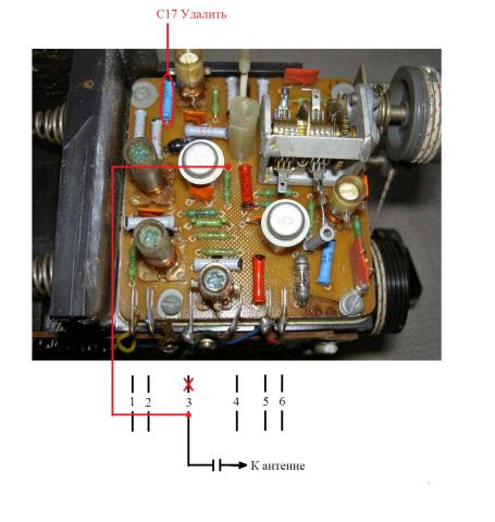
The reconfigured VHF unit works as follows: the received signal is fed to the input of the mixer and at the same time to the local oscillator, where an intermediate frequency (IF) signal is extracted from it, which is fed to terminal "5" of the VHF unit. With the help of a variable capacitor (CPE) C21, the heterodyne circuit is rebuilt from one station to another.
When the receiver is reconfigured in this way, the “Mirror channel” effect is observed, which manifests itself in the form of double overlapping of the range (the same station is received at different KPI positions). This seems to be because the local oscillator, due to its inaccurate tuning, generates frequencies that can extract twice the IF from the same signal. In the first case, the IF is allocated as a frequency difference F signal - F heterodyne = 10.7 MHz, and in the second F heterodyne - F signal = 10.7 MHz. In addition, it should be remembered that the reconfigured block does not have an input circuit (it is simply not used) and a UHF circuit that emits a signal of only one frequency (it is also not used). Only the local oscillator-mixer works, to which the entire frequency band is fed. Therefore, stations located close to each other (in frequency) will interrupt each other when receiving, which complicates the tuning of the receiver. The APCG system (automatic tuning of the local oscillator frequency) will also turn out to be useless, which will work only with powerful stations, and when receiving weak and remote stations, it is recommended to turn off the APCG system and adjust the receiver manually. This is the "price" that you have to pay, abandoning the old VHF band.
In general, the FM receiver works satisfactorily.
We advise you to read
, diagnosis, treatment Treatment of urogenital chlamydia") Chlamydia urogenital - description, causes, symptoms (signs), diagnosis, treatment Treatment of urogenital chlamydia
Chlamydia urogenital - description, causes, symptoms (signs), diagnosis, treatment Treatment of urogenital chlamydia The benefits and significance of hydroamino acid threonine for the human body L threonine what
 To wait or not to wait for a guy from the army For what reason can they be commissioned from the army
 Baked apples with cottage cheese Baked apples with cottage cheese